


方案详情
文
X光检测系统是PCB和半导体器件质量控制、成品率提高和失效分析的关键工具。在许多情况下,这些强大的工具提供了检查电子元件的唯一无损技术。在过去的几年中,X光检查能力(2D和3D)有了显著的改进。在本文中,我们报道了一种新的发展,允许通过二维x射线检查获得材料和厚度信息。
方案详情

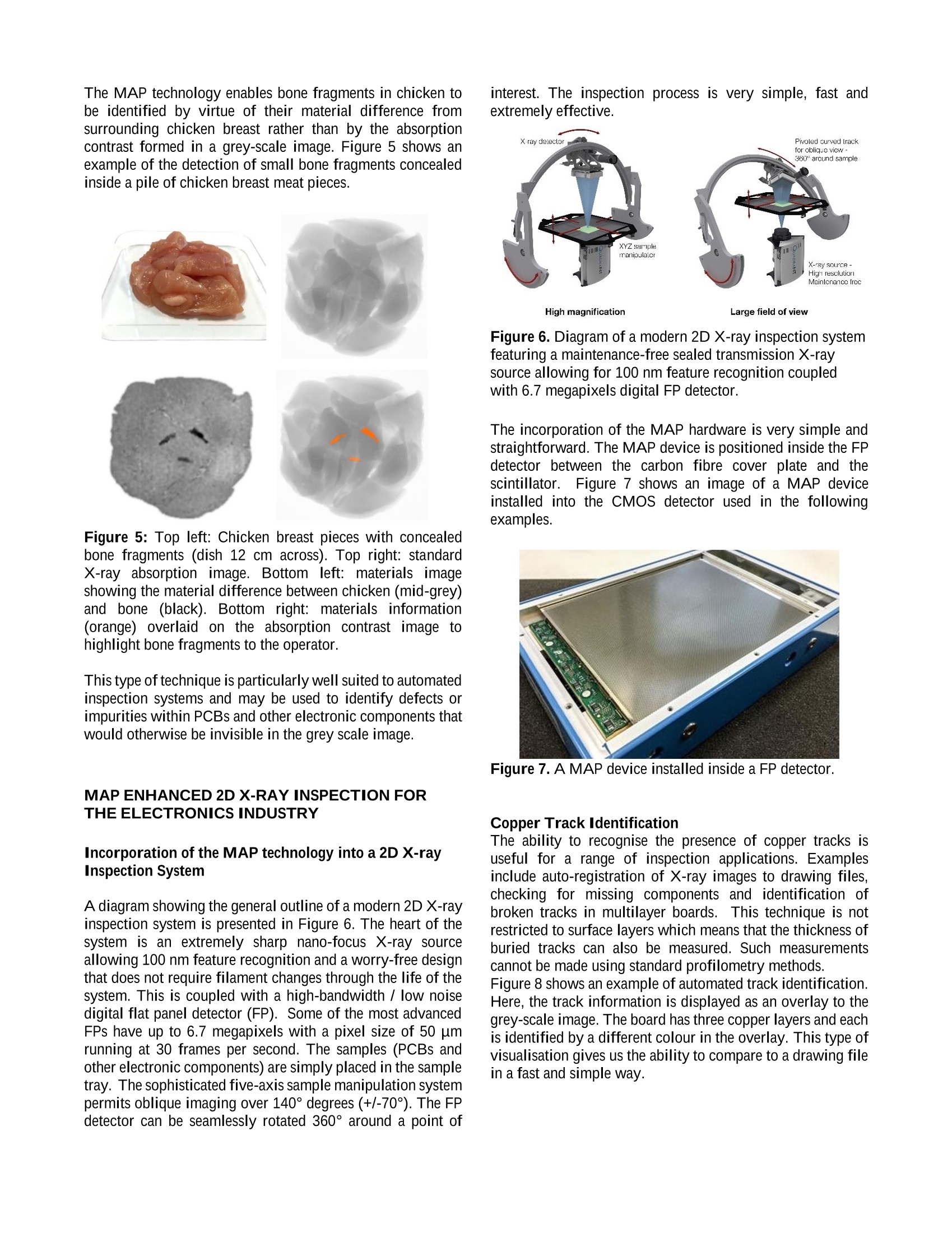
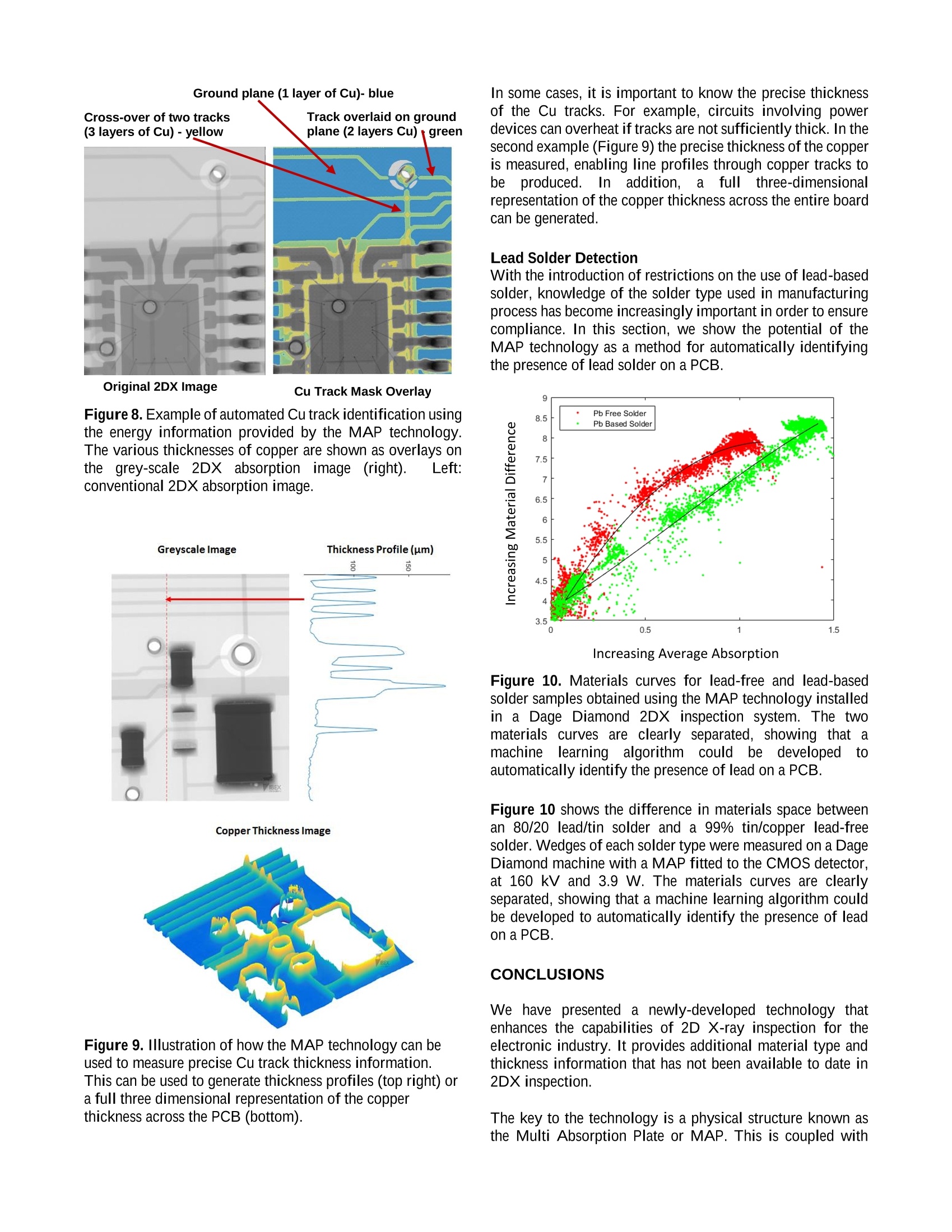
2D X-RAYINSPECTION WITH MATERIALS AND THICKNESSIDENTIFICATION P.D.Scott, Ph.D. IBEX Innovations Sedgefield, County Durham, UK p.scott@ibexinnovations.co.uk Evstatin Krastev, Ph.D.,P.E.Nordson Dage Aylesbury, Buckinghamshire, UKevstatin.krastev@nordsondage.com X-ray inspection systems are key tools for quality control,yield enhancement, and failure analysis of PCBs andsemiconductor devices. In many cases, these capable toolsprovide the only non-destructive techniques for inspection ofelectroniccomponents.There hhavebeensignificantimprovements in the X-ray inspection capabilities (both 2Dand 3D) in the last several years. In this paper we report anew development that permits material and thicknessinformation to be obtained via 2D X-ray inspection. While absorption contrast X-ray imaging is a very powerfulinspection technique, it does not exploit all of the informationpresent within the X-ray beam transmitted through a sample.A new technology has been recently developed that, insteadof simply measuring the total absorption of the X-ray beam,also enables changes in the beam energy to be resolved. Thisallows the effects of thickness and density to be decoupled,enablingg bothtobedetermined.Thisquantitativecomposition and thickness information can then be used toprovide new levels of insight in PCB and semiconductorinspection, potentially leading the way to a new generation ofX-ray inspection technology. It is quite straightforward to accommodate this technology inan existing 2D X-ray (2DX) inspection system. Advancedsoftware algorithms need to be incorporated and an intuitiveuser interface is provided. We present an overview of this new technology and giveexamples of other industries where this technology is beingadopted, as well as example applications for the PCB andsemiconductor industries. Keywords: X-ray inspection, 2DX, 3D CT, AXI, MultiAbsorption Plate, MAP, PCB inspection, materialidentification, thickness identification, profilometry,automated X-ray inspection, X-ray technology,PCT, CTwithout cutting, Large Board CT, non-destructive. The need to inspect electronic components and assembliesnon-destructively is the main driver behind the developmentand advancement of the X-ray inspection technology for theelectronics industry. In many cases, X-Ray inspection (2Dand 3D) provides the only non-destructive techniques toinspect optically hidden components and solder joints such asBGA, POP, QFN, flip chips, through holes, TSVs, micro-bumps, copper pillars, etc. All X-ray inspection systems (2D and 3D) rely on absorptioncontrast imaging, where the contrast is generated by thestopping power of the sample. As such, higher density and/orthicker regions of a sample produce darker regions in a grey-scale image.X-ray inspection systems use this method toimage features such as wire bonds and ball grid arrays downto a feature recognition size of 100 nm(0.1 um). While contrast imaging is a very powerful and widely usedtechnique, there is significantly more information presentwithin the X-ray beam, which, until now, has not beenexploited in electronics inspection. Instead of simplymeasuring the total absorption of the X-ray beam, a physicalstructure known as a Multi Absorption Plate (MAP) can beplaced in the beam path. This, coupled with machine learningalgorithms, enables material type and thickness informationto be acquired alongside the standard grey-scale image. Quantitative composition and thickness information can thenbe used to provide more detailed diagnostics in PCB andsemiconductor inspection. Applications include, but are notlimitedtto, analysiss of solderr types, trackthicknessmeasurements, and conformance to quality standards. An overview of the theory behind the operation of the MAPis given below, as well as some simple examples showing thebenefits of using the MAP technology to add additionalcapabilities to 2D X-Ray inspection. MAP technology alsohas applications in the security, medical and food processingindustries. Nordson Dage has partnered with IBEX to bring the benefits of this technology to the electronics inspection,including inspection of PCBs and semiconductor devices. Arange of examples is presented and the authors aim to startactive discussions that would generate new needs and ideasfor use of the technology for non-destructive inspection ofelectronics systems and components. BASIC PRINCIPLES OF THE MAP TECHNOLOGY X-ray Interaction with a Sample X-rays are generated using a tungsten target which producesa continuous spectrum, known as BremBtrahlung radiation,as well as characteristic peaks at specific energies. Adding a sample such as a printed circuit board into the beamattenuates the X-ray spectrum in the following way: where I(E) andI(E) are the intensities of the X-ray spectrabefore and after the sample, respectively, u(E) is thematerial-dependent linear attenuation coefficient and t is thethickness of the sample. If I(E) and I(E) can be determined, it is possible to extractthe parameter u(E) which relates to the material type and thematerial thickness. A standard CMOS detector integrates the total energydeposited into each pixel over the user-selected integrationtime. As such, the detector is able to measure total energydeposited per pixel but not the actual energy spectrum. Thismeans that it is not possible to decouple the material andthickness terms in equation (1), meaning that thin, highdensity materials are indistinguishable from thick, lowdensity materials in a single 2D projection. The Multi Absorption Plate (MAP) acts like a complex“colour” filter for the X-rays by imposing a repeatingmodulation to the X-ray beam over a few neighbouringpixels. This modulation results in a variation in the energydistribution of the X-ray beam incident on the neighbouringpixels in a way that enables unique materials information tobe obtained. Extracting Materials Information -Simple Examples Figure 1 shows the word IBEX constructed using a series ofcopper tiles with a background made up of foils of silver. Thethicknesses of the foils have been selected in order torandomise the grey-scale intensity transmitted by the tiles andhence obscure the word IBEX in a standard X-ray image.Analysing the image with a MAP in place recovers thematerials information. The intensities of the colouring in thebottom image of Figure 1 reflect the relative thicknesses ofthe tiles. Figure 1. Optical image showing the word IBEX created asa mosaic of random thicknesses of silver and copper foils(top); X-ray transmission image showing that it is notpossible to distinguish between the foils using absorptioncontrast alone (middle); materials contrast image showingthat the missing information can be recovered using the MAP(bottom). This materials information can be displayed to the user interms of a basic mask identifying the materials, as an overlayof material identification on the absorption contrast image, orin the case of automated quality inspection systems as apass/fail criterion. Figure 2.“Materials curves” (left) generated from trainingthe system on the wedge samples (right). Decisions on material type are made by reference to a“materials space” plot. The position of a point in this plotgives information on both the material type and thickness. Anexample is shown in Figure 2 for wedges of aluminium, ironand PMMA. MACHINE LEARNING/USER INTERFACE Machine learning algorithms have been developed to enabledecisions to be made on material type and thickness based onthe materials space plots generated from the image obtained using the MAP.The algorithms require training using a set oftraining standards. Once the training stage is complete, thealgorithm is able to identify the material and thickness ofpreviously unseen samples. Under ideal test conditions, thealgorithm has been shown to have a misclassification rate ofless than 2% and is able to identify thickness to better than1% of the true value. Once the MAP has been fitted to the CMOS detector, thecalibration, database training and sample analysis are handledby a simple user interface which is integrated into the X-rayinspection system software. An example is shown inFigure 3 where wedges of three materials are trained and usedto identify the material types on the right of the image. Figure 3. Screen shots showing a user interface which isdesigned to allow materials training (top) and identification(bottom). The algorithm works at a rate compatible with imageacquisition times and generates a standard grey-scale imageas part of the process. EXAMPLE APPLICATIONS This article is focussed on discussing the X-ray MAPinspection technology for the electronics industry, includingPCBs and semiconductor applications. In this section, weshow some examples of the MAP X-ray inspectiontechnology applied in the security and food industries. Theintention is to enhance the reader’s understanding of thetechnology and to facilitate the generation of ideas andrequirements that can apply for the electronics industry. Security Inspection Security threats may be disguised within everyday objectssuch as laptops and mobile telephones, which are legitimatelycarried. X-ray security scanners typically use measurementstaken at two voltage settings of the X-ray generator in orderto generate materials information. This approach requires twoscans. Using the MAP, the measurement can be reduced to asingle scan at only one voltage setting. A desk telephone, shown in Figure 4, was measured as an example of a complex objectcontaining electronic circuitry and plastics. Datawerecollected at 120 kV, 0.5 mA, with a 0.5 s exposure, using aconventional, low-power tungsten X-ray source and a siliconflat-panel detector equipped with the MAP technology.Analysis of the image dataleadsto the materialsdiscrimination image shown in Figure 4 (right). The colour-scheme here is one typically used in security applications:plastics and other organic materials are presented in orange;so called “poor”metals, such as aluminium, are shown ingreen; denser metals are shown in blue. Figure 4. Left: Absorption contrast image of a telephone.Right: Materials contrast image showing plastics (orange),“poor”metals (green) and dense metals (blue). We see the potential for the same techniques to be applied inPCB inspection to highlight inconsistencies in circuit boardsand other electronic components. Food Inspection Detecting bone fragments in meat products is just one aspectof food safety which is important to both consumers and foodproducers. Fresh meat products pose particular challenges:the sample shape is not regular and there is variation fromone sample to the next; the thickness of the product varies;the bone fragments are probably not visible on the outside ofthe sample; and the bone fragments are small compared to thesurrounding flesh. X-ray absorption contrast and imagerecognition techniques have limited application in this fieldas the bone fragments have a very similar X-ray absorptionsignature to the meat, resulting in edges and shapes thatcrestonannot be clearly identified (Figure 5 top right). The MAP technology enables bone fragments in chicken tobe identified by virtue of their material difference fromsurrounding chicken breast rather than by the absorptioncontrast formed in a grey-scale image. Figure5 shows anexample of the detection of small bone fragments concealedinside a pile of chicken breast meat pieces. Figure 5: Top left: Chicken breast pieces with concealedbone fragments (dish 12 cm across). Top right: standardX-ray absorption image. Bottomleft: materials; imageshowing the material difference between chicken (mid-grey)and bone (black). Bottom right: materials information(orange) overlaid on the absorption contrast image tohighlight bone fragments to the operator. This type of technique is particularly well suited to automatedinspection systems and may be used to identify defects orimpurities within PCBs and other electronic components thatwould otherwise be invisible in the grey scale image. MAP ENHANCED 2D X-RAY INSPECTIONFORTHE ELECTRONICS INDUSTRY Incorporation of the MAP technology into a 2D X-rayInspection System A diagram showing the general outline of a modern 2D X-rayinspection system is presented in Figure 6. The heart of thesystem is an extremely sharp nano-focus X-ray sourceallowing 100 nm feature recognition and a worry-free designthat does not require filament changes through the life of thesystem. This is coupled with a high-bandwidth / low noisedigital flat panel detector (FP). Some of the most advancedFPs have up to 6.7 megapixels with a pixel size of 50 umrunning at 30 frames per second. The samples (PCBs andother electronic components) are simply placed in the sampletray. The sophisticated five-axis sample manipulation systempermits oblique imaging over 140° degrees (+/-70). The FPdetector can be seamlessly rotated 360° around a point of interest. The inspection process is very simple, fast andextremely effective. Figure 6. Diagram of a modern 2D X-ray inspection systemfeaturing a maintenance-free sealed transmission X-raysource allowing for 100 nm feature recognition coupledwith 6.7 megapixels digital FP detector. The incorporation of the MAP hardware is very simple andstraightforward. The MAP device is positioned inside the FPdetector between the carbon fibre cover plate and thescintillator. Figure 7 shows an image of a MAP deviceinstalled into the CMOS detector used in the followingexamples. Figure 7. A MAP device installed inside a FP detector. Copper Track Identification The ability to recognise the presence of copper tracks isuseful for a range of inspection applications. Examplesinclude auto-registration of X-ray images to drawing files,checking for missing components and identification ofbroken tracks in multilayer boards.S.TThis technique is notrestricted to surface layers which means that the thickness ofburied tracks can also be measured. Such measurementscannot be made using standard profilometry methods. Figure 8 shows an example of automated track identification.Here, the track information is displayed as an overlay to thegrey-scale image. The board has three copper layers and eachis identified by a different colour in the overlay. This type ofvisualisation gives us the ability to compare to a drawing filein a fast and simple way. Ground plane (1 layer of Cu)-blue Cross-over of two tracks Track overlaid on ground Original 2DX Image Cu Track Mask Overlay Figure 8. Example ofautomated Cu track identification usingthe energy information provided by the MAP technology.The various thicknesses of copper are shown as overlays onthe grey-scale2DXabsorption image (right). Left:conventional 2DX absorption image. Figure 9. Illustration of how the MAP technology can beused to measure precise Cu track thickness information.This can be used to generate thickness profiles (top right) ora full three dimensional representation of the copperthickness across the PCB (bottom). In some cases, it is important to know the precise thicknessof the Cu tracks. For example, circuits involving powerdevices can overheat if tracks are not sufficiently thick. In thesecond example (Figure 9) the precise thickness of the copperis measured, enabling line profiles through copper tracks tobe produced. In addition.a full three-dimensionalrepresentation of the copper thickness across the entire boardcan be generated. Lead Solder Detection With the introduction of restrictions on the use oflead-basedsolder, knowledge of the solder type used in manufacturingprocess has become increasingly important in order to ensurecompliance. In this section, we show the potential of theMAP technology as a method for automatically identifyingthe presence of lead solder on a PCB. Increasing Average Absorption Figure 10. Materials curves for lead-free and lead-basedsolder samples obtained using the MAP technology installedin ia Dage Diamond 2DX inspection system. The twomaterials curves are clearly separated, showing thatamachine learning algorithm couldd be ddevelopedautomatically identify the presence of lead on a PCB. Figure 10 shows the difference in materials space betweenan 80/20 lead/tin solder and a 99%tin/copper lead-freesolder. Wedges ofeach solder type were measured on a DageDiamond machine with a MAP fitted to the CMOS detector,at 160 kV and 3.9 W. The materials curves are clearlyseparated, showing that a machine learning algorithm couldbe developed to automatically identify the presence of leadon a PCB. CONCLUSIONS We have presented a newly-developed technology thatenhances the capabilities of 2D X-ray inspection for theelectronic industry. It provides additional material type andthickness information that has not been available to date in2DX inspection. The key to the technology is a physical structure known asthe Multi Absorption Plate or MAP. This is coupled with sophisticated machine learning algorithms and trainingmethodologies. Several cases were discussed to demonstrateapplications in the electronics, security and food safetyindustries. Below are key enhancements gained throughMAP technology: Enables users to visualise samples in a new way bylooking at a materials image as well as a standardgrey-scale absorption contrast image. Detection of defects and impurities that are invisiblein the regular 2DX grey-scale image. Quantitative thicknessand material informationreturned to the user. Can be fitted to most flat panel detectors. Near real-time operation. Ability to adapt algorithms for automated inspectionapplications. The authors are very interested in discussions,.. ideas andcollaborations within the electronics industry in order tofocus the developments and take full advantage of this new,exciting technology. ACKNOWLEDGEMENTS The authors would like to thank Tamzin Lafford for her greathelp during the final stages of the paper development! REFERENCES ( [1] Evstatin Krastev and John Tingay, Recent Advances In T he X-Ray Inspection Technology With Emphasis On Large Board Computer Tomography And Automation,PanPac M icroelectronics Symposium 2014. ) ( [2] Evstatin Krastev , D . Bernard, Dragos Golubovic, 3DBoard level X -ray i n spection v i a limited angle computer tomography, SMTAI conference 2012. ) ( [3] S. Sethuraman et al., The Effect of Process Voiding on BGA Solder Joint F a tigue Life Measured in AcceleratedThermal C ycling, SMTAI conference 2007. ) ( [4]D.Hillman et al., T he Last Will and T e stament of the BGA Void, SMTAI conference 2011. ) ( [5] G. Qin et sG. al., Assessing the Impac t of Temperature Cycling Reliability of High Levels of Voiding in BGA Solder Joints , SMTAI conference 2012. ) ( [6] Evstatin Krastev & D. Bernard,Modern 2d /3d X - rayInspection-Emphasis on BGA, QFN,3d Pa c kages, and Counterfeit Components, Pan Pacific SymposiumConference Proceedings 2010 ) ( [7] Zhen ( Jane) F eng, Ph.D., Juan C a rlos Gonzalez, Sea T ang, Murad Kurwa, and Evstatin Krastev, Non-Destructive ) Techniques For Identifying Defect In BGA Joints: TDR,2DX, And Cross-Section/SEM Comparison,,SMTAIconference 2008. X光检测系统是PCB和半导体器件质量控制、成品率提高和失效分析的关键工具。在许多情况下,这些强大的工具提供了检查电子元件的唯一无损技术。在过去的几年中,X光检查能力(2D和3D)有了显著的改进。在本文中,我们报道了一种新的发展,允许通过二维x射线检查获得材料和厚度信息。
确定


还剩4页未读,是否继续阅读?

产品配置单
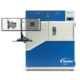


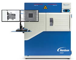
聚擘国际贸易(上海)有限公司为您提供《PCB中材料、厚度检测方案(X射线成像)》,该方案主要用于电子元器件产品中材料、厚度检测,参考标准--,《PCB中材料、厚度检测方案(X射线成像)》用到的仪器有DAGE X光检测系统Quadra 7、DAGE X光检测系统Quadra 5、DAGE X光检测系统Quadra 7、DAGE X光检测系统Quadra 5
相关方案
更多
该厂商其他方案
更多