


方案详情
文
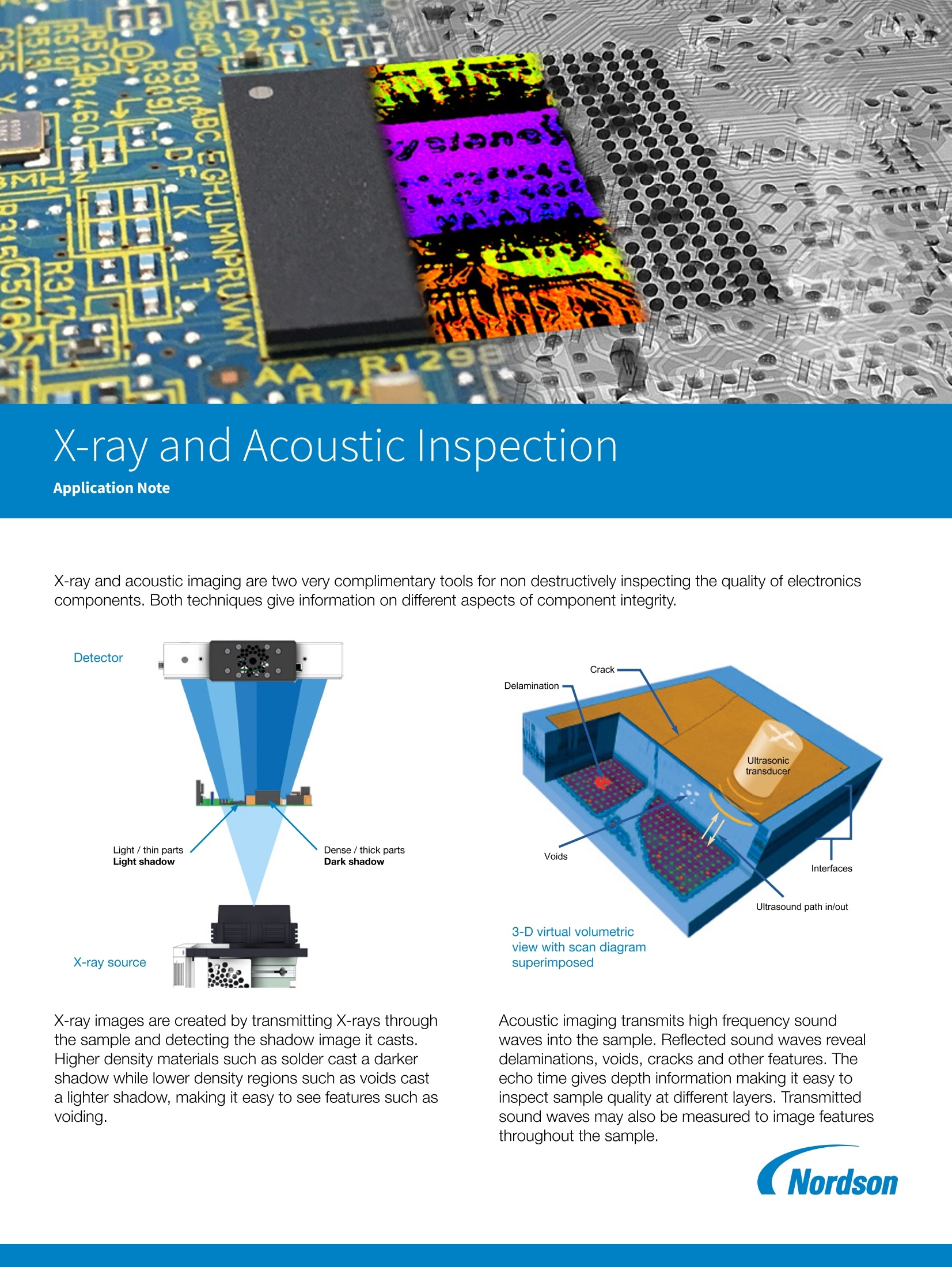
X光无损检测及超声波无损检测应用手册 X光和超声波成像是两个非常有益的工具,用于无损检测电子组件产品的质量。这两种技术都提供了关于组件完整性的不同方面的信息。
方案详情

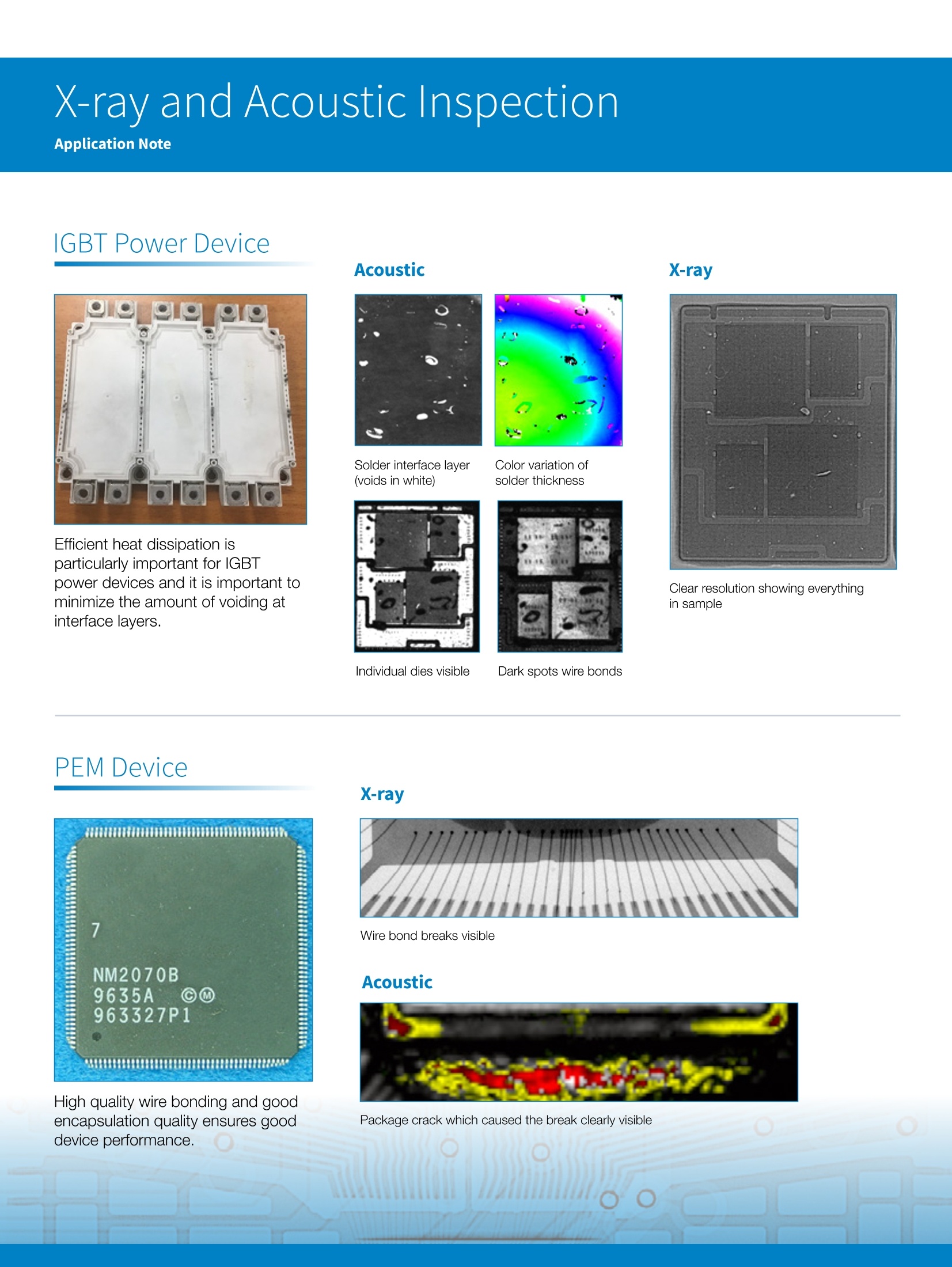
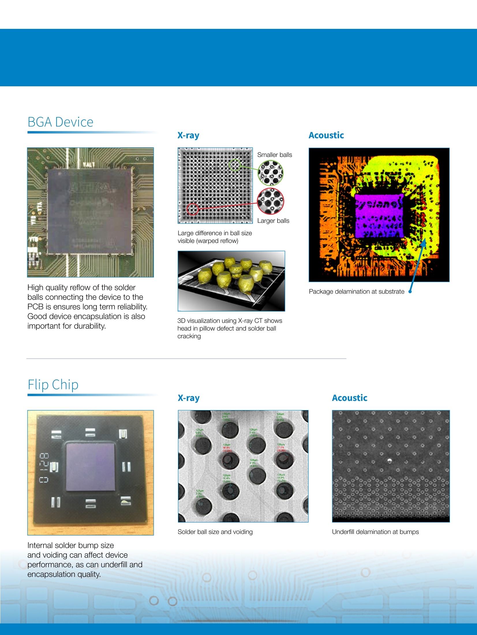
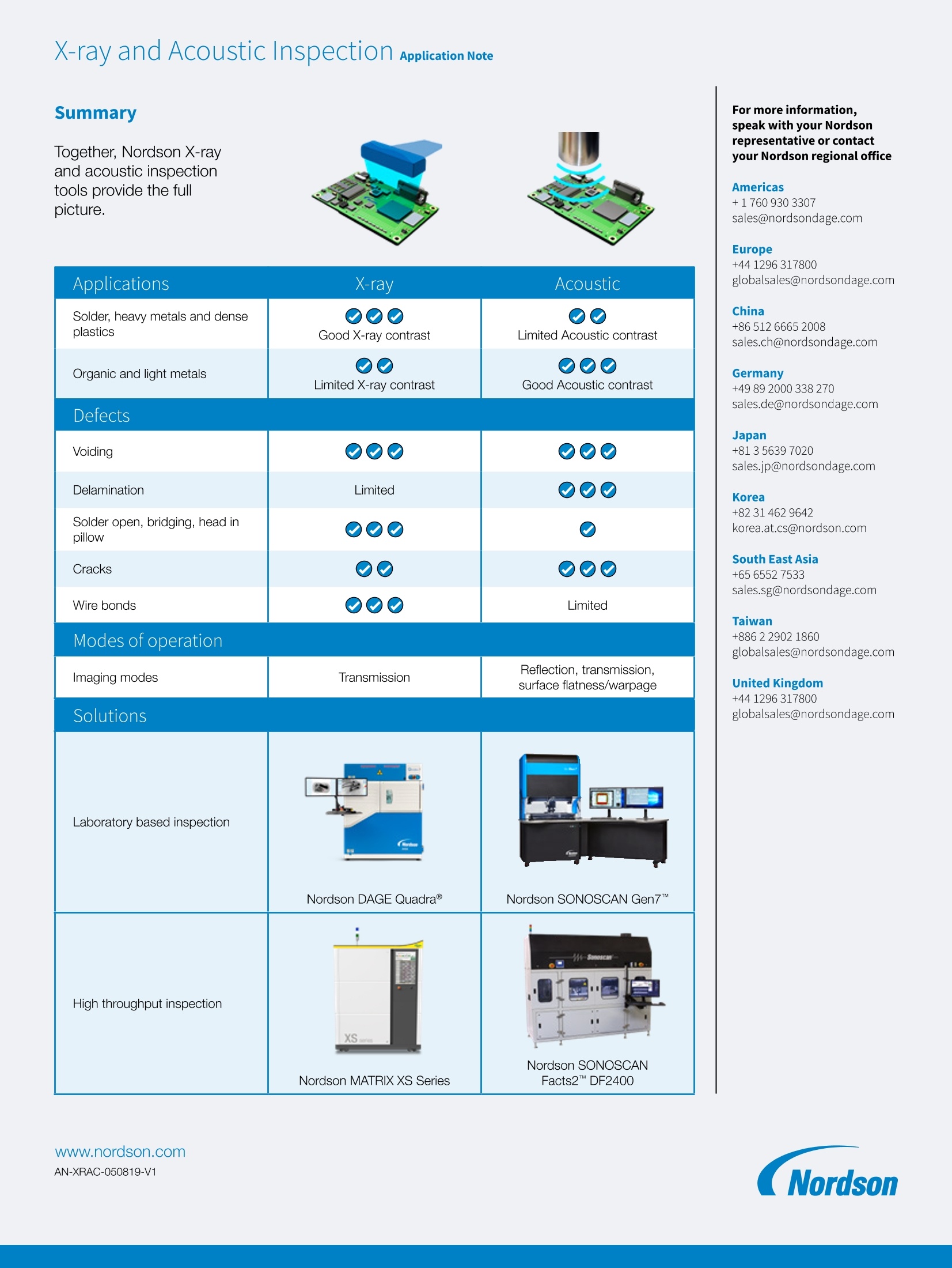
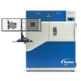
Application Note BGA Device www.nordson.comAN-XRAC-050819-V1 122 4309/ UR310A0 lS1 MI ! A R1298 R7 X-ray and Acoustic InspectionApplication Note X-ray and acoustic imaging are two very complimentary tools for non destructively inspecting the quality of electronicscomponents. Both techniques give information on different aspects of component integrity. superimposed X-ray images are created by transmitting X-rays throughthe sample and detecting the shadow image it casts.Higher density materials such as solder cast a darkershadow while lower density regions such as voids casta lighter shadow, making it easy to see features such asvoiding. Acoustic imaging transmits high frequency soundwaves into the sample. Reflected sound waves revealdelaminations, voids, cracks and other features. Theecho time gives depth information making it easy toinspect sample quality at different layers. Transmittedsound waves may also be measured to image featuresthroughout the sample. X-ray and Acoustic Inspection |GBT Power Device Acoustic X-ray Solder interface layer(voids in white) Color variation ofsolder thickness Efficient heat dissipation isparticularly important for IGBTpower devices and it is important tominimize the amount of voiding atinterface layers. Clear resolution showing everythingin sample Individual dies visible Dark spots wire bonds PEM Device X-ray Wire bond breaks visible Acoustic High quality wire bonding and goodencapsulation quality ensures gooddevice pertormance. Package crack which caused the break clearly visible High quality reflow of the solderballs connecting the device to thePCB is ensures long term reliability.Good device encapsulation is alsoimportant for durability. Flip Chip Internal solder bump sizeand voiding can affect deviceperformance, as can underfill andencapsulation quality. Large difference in ball sizevisible (warped reflow) Package delamination at substrate 3D visualization using X-ray CT showshead in pillow defect and solder ballcracking Summary For more information, speak with your Nordson representative or contact Together, Nordson X-rayand acoustic inspectiontools provide the fullpicture. your Nordson regional office Americas 27 +1760930 3307 sales@nordsondage.com Europe +441296317800 Applications X-ray Acoustic globalsales@nordsondage.com China Solder, heavy metals and dense +86 512 6665 2008 plastics Good X-ray contrast Limited Acoustic contrast sales.ch@nordsondage.com Organic and light metals Germany Limited X-ray contrast Good Acoustic contrast +49 892000 338270 sales.de@nordsondage.com Defects Japan Voiding +813 56397020 sales.jp@nordsondage.com Delamination Limited Korea +82314629642 Solder open, bridging, head in O D korea.at.cs@nordson.com pillow South East Asia Cracks +6565527533 sales.sg@nordsondage.com Wire bonds Limited Taiwan Modes of operation +886 2 29021860 globalsales@nordsondage.com Reflection, transmission, lmaging modes Transmission surface flatness/warpage United Kingdom +44 1296317800 Solutions globalsales@nordsondage.com Laboratory based inspection Nordson DAGE Quadra Nordson SONOSCAN Gen7 High throughput inspection 11 XS Nordson SONOSCAN Nordson MATRIX XS Series Facts2DF2400 X光无损检测及超声波无损检测应用手册 X光和超声波成像是两个非常有益的工具,用于无损检测电子组件产品的质量。这两种技术都提供了关于组件完整性的不同方面的信息。
确定
还剩2页未读,是否继续阅读?

产品配置单


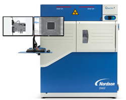
聚擘国际贸易(上海)有限公司为您提供《电子半导体器件中无损检测方案(X射线成像)》,该方案主要用于集成电路中机械性能检测,参考标准--,《电子半导体器件中无损检测方案(X射线成像)》用到的仪器有DAGE X光检测系统Quadra 7、DAGE X光检测系统Quadra 5、DAGE X光检测系统Quadra 7、DAGE X光检测系统Quadra 5、Sonoscan超声波扫描显微镜