


方案详情
文
采用立陶宛Ekspla公司生产的纳秒短脉冲半导体泵浦的固体激光器-NL220.波长532nm.脉冲宽度35纳秒,重复频率500Hz.处理ITO玻璃上3-30nm厚的镀金薄膜。生成纳米颗粒,具有独特的电化学特性,可以用来制作电化学传感器。
方案详情

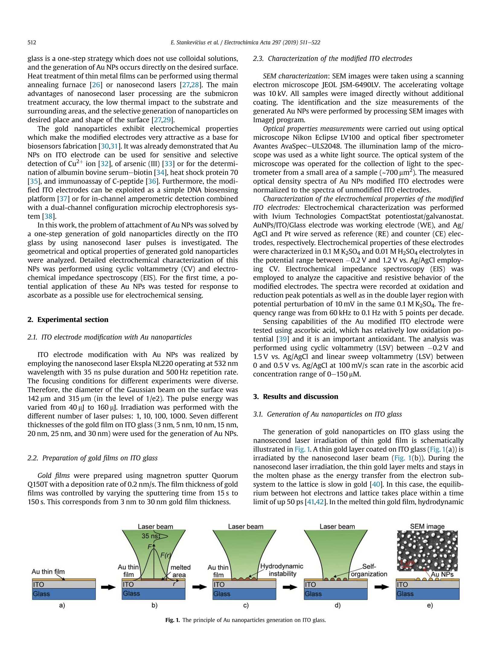
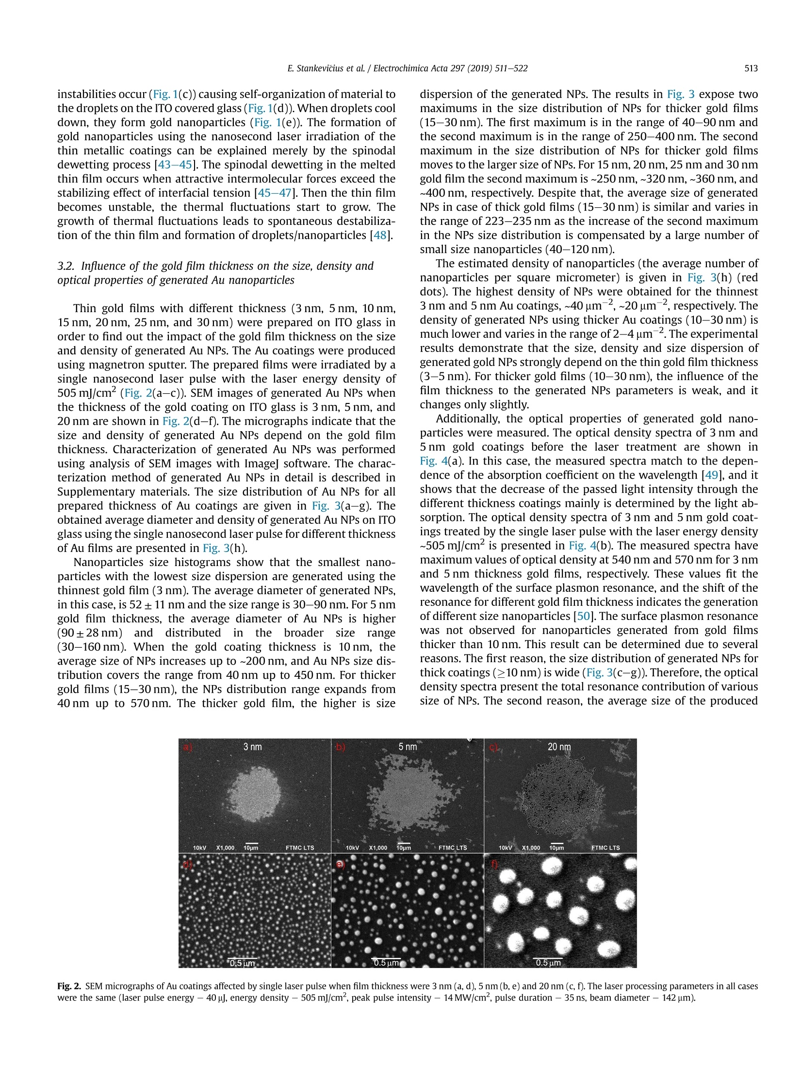
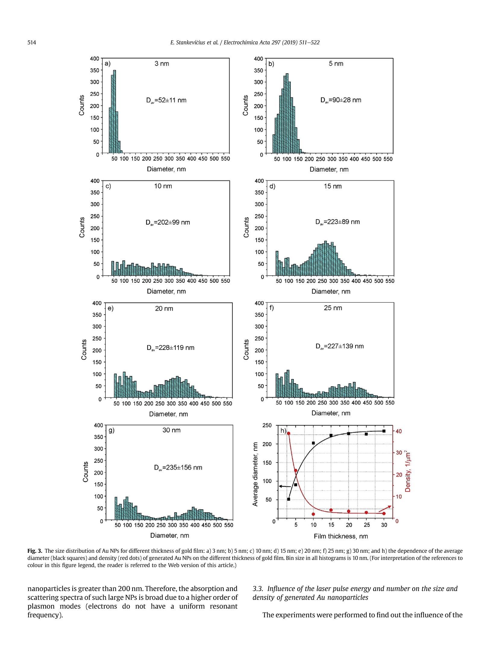
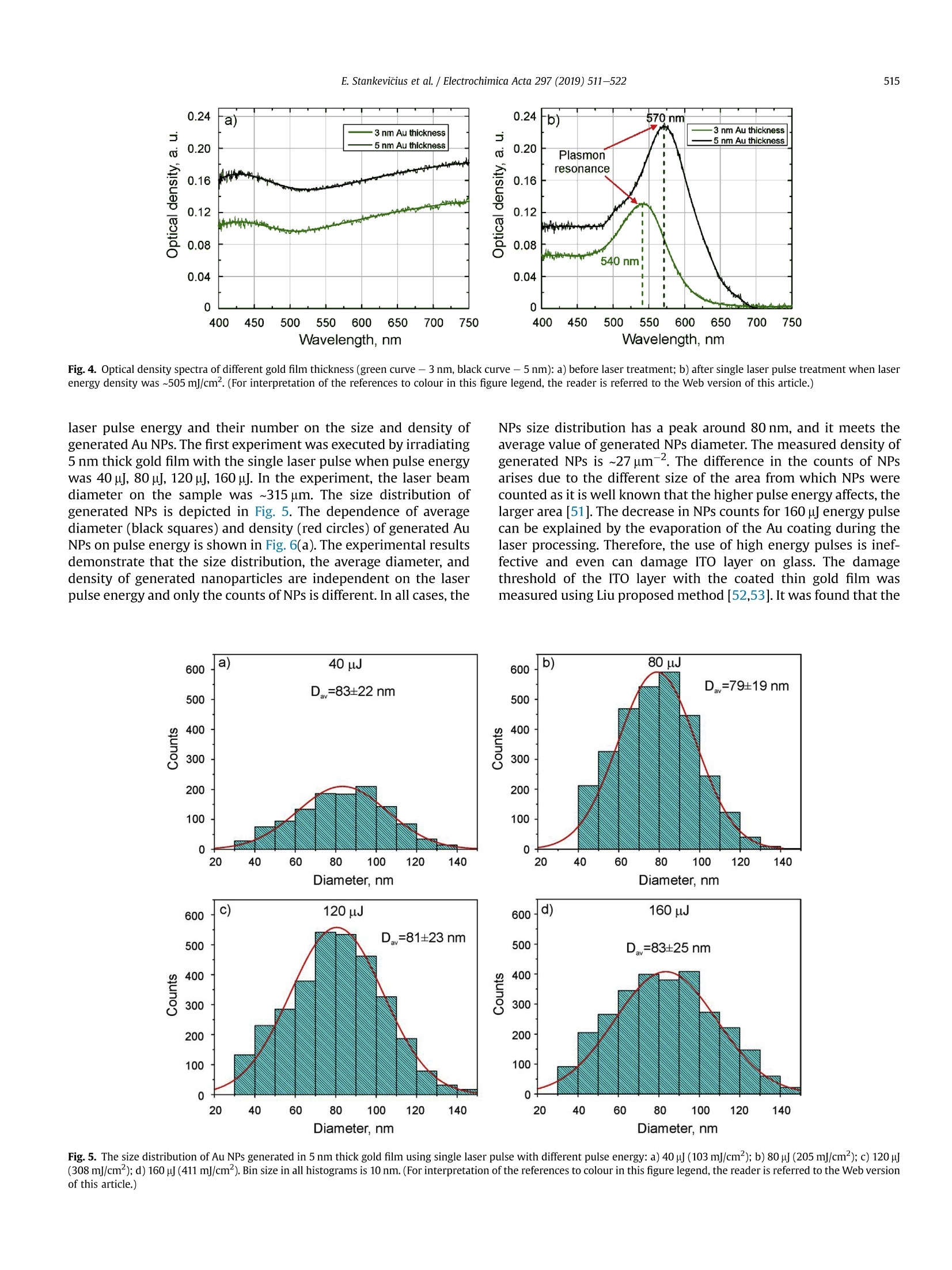
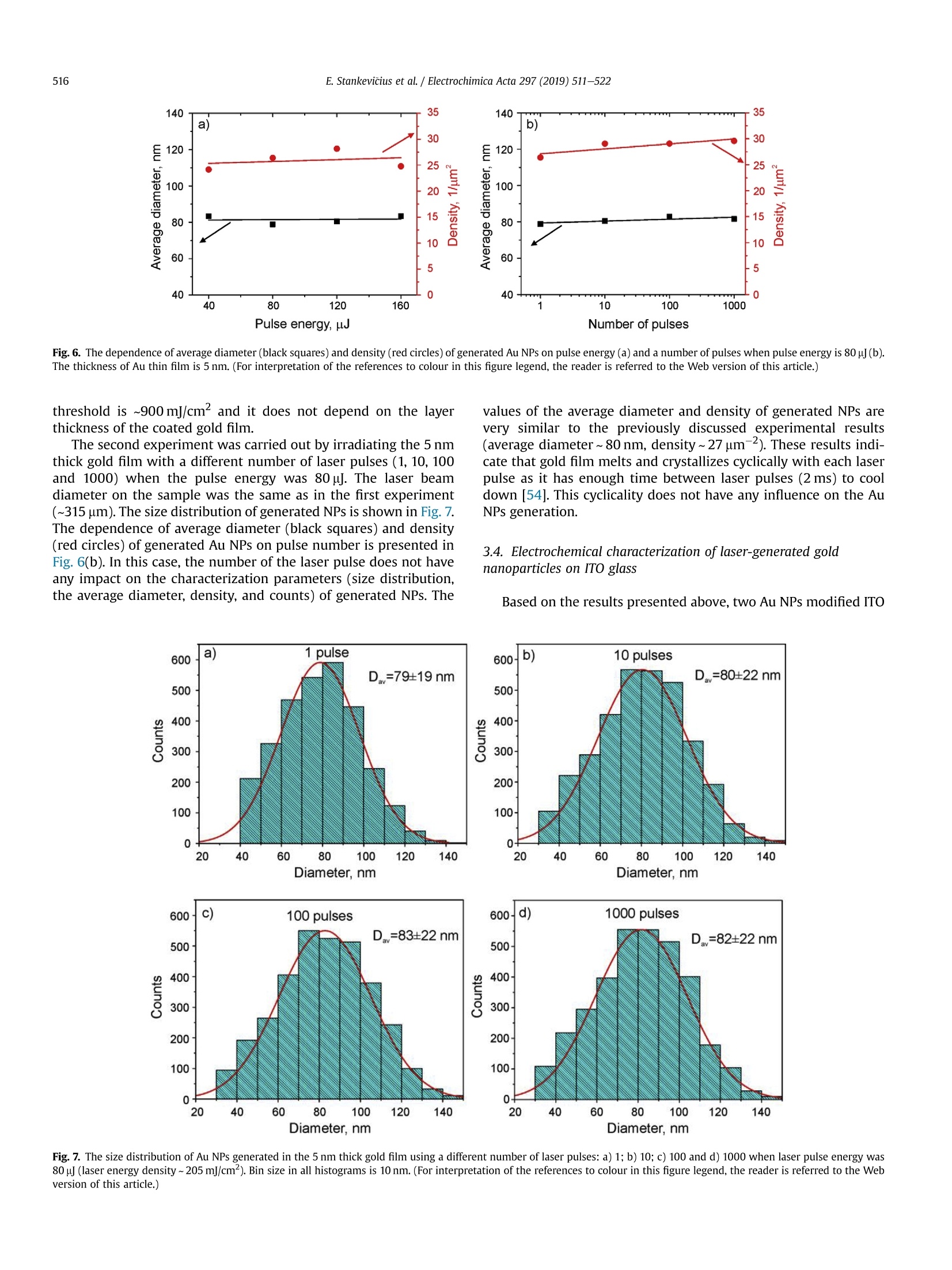
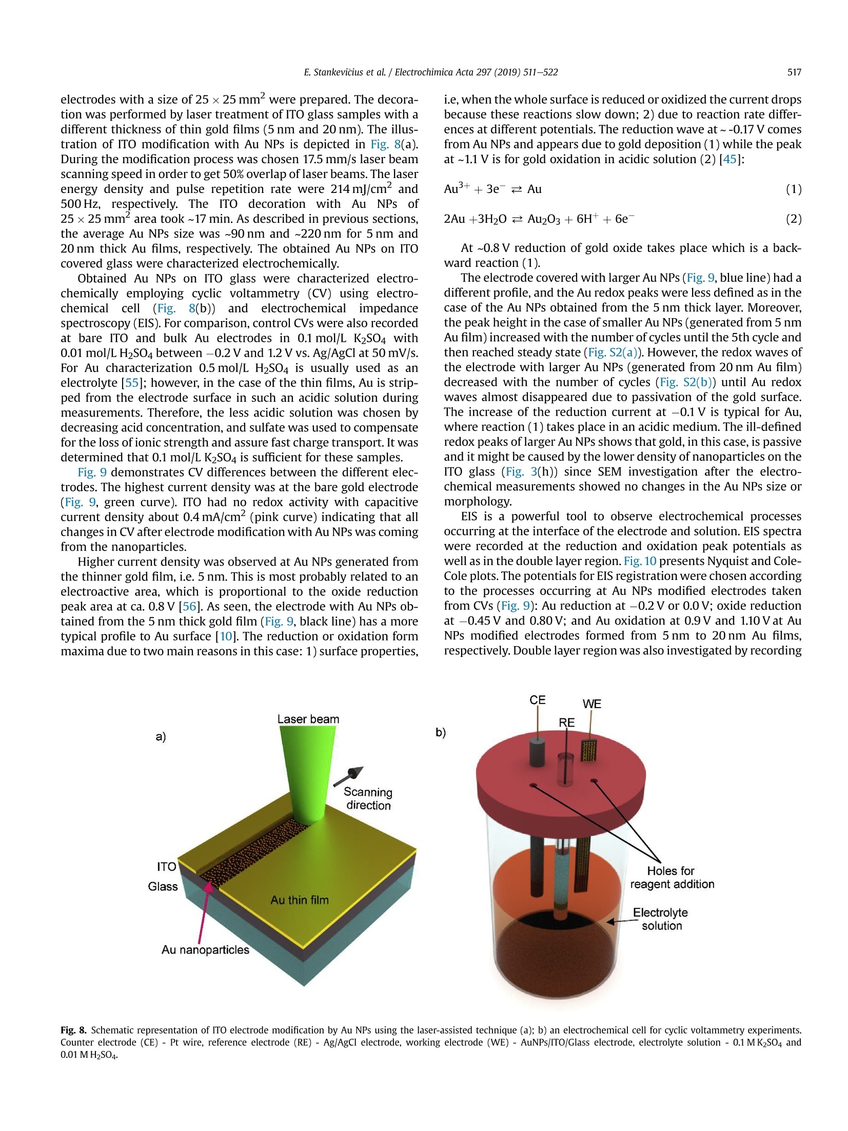
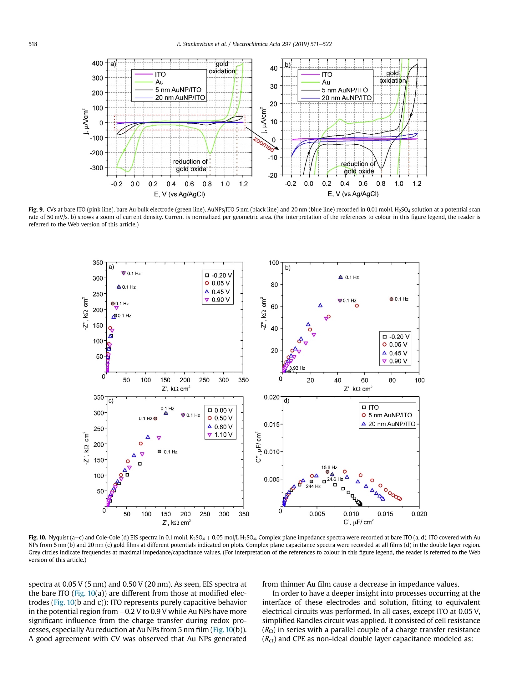
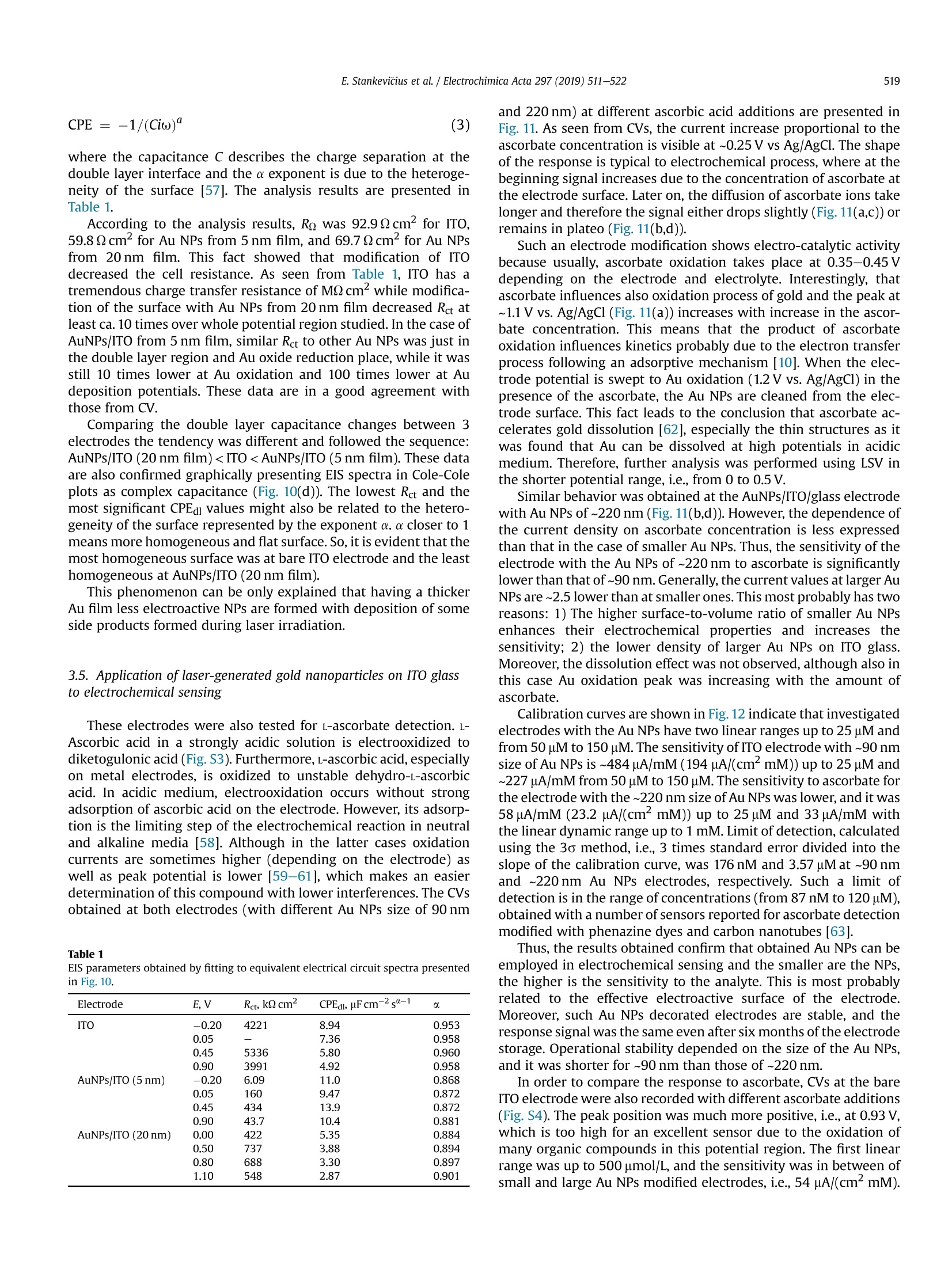
Electrochimica Acta 297 (2019)511-522 512E. Stankevicius et al./Electrochimica Acta 297 (2019) 511-522 0013-4686/@ 2018 The Authors. Published by Elsevier Ltd. This is an open access article under the CC BY-NC-ND license (http://creativecommons.org/licenses/by-nc-nd/4.0/). Contents lists available at ScienceDirect Electrochimica Acta ELSEVIER j ournal homepage: www.elsevier.com/locate/electacta Engineering electrochemical sensors using nanosecond lasertreatment of thin gold film on ITO glass Evaldas Stankevicius a*, Mantas Garliauskas, Lukas Laurinavicius ,Romualdas Trusovas, Nikolai Tarasenko, Rasa Pauliukaite a Center for Physical Sciences and Technology, Savanoriu Av. 231, LT-02300, Vilnius, Lithuania "Stepanov Institute of Physics of National Academy of Sciences of Belarus, Nezavisimosti Ave. 68, 220072, Minsk, Belarus ARTICLEIN F O ABSTRACT Article history: Received 5 October 2018 Received in revised form 22 November 2018 Accepted 28 November 2018 Available online 3 December 2018 Keywords: Gold nanoparticles Nanosecond lasers Thin gold films Heat treatment Cyclic voltammetry Direct generation of gold nanoparticles on ITO glass using a nanosecond laser is presented and theelectrochemical properties of the gold modified ITO electrodes for detection of the ascorbic acid areanalyzed. Gold nanoparticles were generated by nanosecond laser pulse irradiation of thin, 3-30 nmthick, gold films. It was found that diameters and the number of generated nanoparticles per unit areastrongly depends on the thickness of the gold film when it is less than 10 nm. Furthermore, experimentshave shown that the influence of laser processing parameters (the laser pulse energy and pulse number)to the size, the distribution and the area density of generated gold nanoparticles on ITO glass is negli-gible. Characterization of the electrochemical properties of the gold modified ITO electrodes by nano-second laser showed that the fabricated electrodes could be employed in electrochemical sensing.Therefore, the demonstrated generation of gold nanoparticles on ITO by using the nanosecond laserapproach opens new opportunities for the development of highly sensitive and low-cost electrochemicalsensors. Electrochemical impedance spectroscopy o2018 The Authors. Published by Elsevier Ltd. This is an open access article under the CC BY-NC-ND 1. Introduction In electrochemistry, metal nanoparticles are widely utilized as afunctional unit to modify electrode surfaces [1-6] in order todevelop (bio)sensors and energy production cells [7,8] as well as forenvironmental applications [9,10]. Metal nanoparticles providefour main advantages over macroelectrodes for electroanalysis: 1)enhancement of mass transport,2) catalysis,3) high effective sur-face area, and 4) control over local microenvironment [11]. Nano-sized noble metal particles become important for variousapplication fields including biosensors, nanosensors, nanodevices,catalysis, and nanoelectrochemistry [12-15]. Particular interestsare focused on the synthesis and application of gold nanoparticles(Au NPs) in the electroanalytical and electrocatalytic field due tothe ability to enhance the electrode conductivity of the electrodesurface and facilitate the electron transfer, thus, improving theanalytical selectivity and sensitivity [16]. Indium tin oxide (ITO) films on glass or quartz substrates are ( * Corresponding author. ) ( E-mail address: e stankevici u s @ft m c.lt ( E. S tankevicius). ) often used as electrodes surface due to their prominent charac-teristics such as an excellent electrical conductivity and wideelectrochemical working window [17,18], as well as low-cost [16].ITO electrode modified with Au NPs possesses a faster electrontransfer rate and larger current response than the bare ITO elec-trode [19]. Therefore, such electrodes can be applied for the crea-tion of highly sensitive and selective future sensors. Themodification of ITO electrode with Au NPs faces with the problemof the deposition of colloidal nanoparticles on ITO coating. Theimmobilization of Au NPs by using binding molecules such as thiols[20] and silanes [21] is ideal for glass surfaces [22], however, thismethod does not allow to obtain a high coverage of Au NPs on theelectrode surface in the case of ITO coatings. Furthermore, theelectroactivity of the Au NPs films fabricated employing thisapproach is influenced by the contamination of various com-pounds, such as the reactants, surfactant and binder molecules, aswell as these methods have the time-consuming, complex syn-thesis procedures. Other more efficient Au NPs modification of ITO electrodesmethods as centrifugation [23], electrochemical deposition [19],seed-mediated growth process [24,25] or thin film thermal treat-ment can be used. Thermal treatment of thin gold coatings on ITO glass is a one-step strategy which does not use colloidal solutions,and the generation of Au NPs occurs directly on the desired surface.Heat treatment of thin metal films can be performed using thermalannealing furnace [26] or nanosecond lasers [27,28]. The mainadvantages of nanosecond laser processing are the submicrontreatment accuracy, the low thermal impact to the substrate andsurrounding areas, and the selective generation of nanoparticles ondesired place and shape of the surface [27,29]. The gold nanoparticles exhibit electrochemical propertieswhich make the modified electrodes very attractive as a base forbiosensors fabrication [30,31]. It was already demonstrated that AuNPs on ITO electrode can be used for sensitive and selectivedetection of Cu²+ ion [32], of arsenic (III) [33] or for the determi-nation of albumin bovine serum-biotin [34], heat shock protein 70[35], and immunoassay of C-peptide [36]. Furthermore, the modi-fied ITO electrodes can be exploited as a simple DNA biosensingplatform [37] or for in-channel amperometric detection combinedwith a dual-channel configuration microchip electrophoresis sys-tem [38]. In this work, the problem of attachment of Au NPs was solved bya one-step generation of gold nanoparticles directly on the ITOglass by using nanosecond laser pulses is investigated. Thegeometrical and optical properties of generated gold nanoparticleswere analyzed. Detailed electrochemical characterization of thisNPs was performed using cyclic voltammetry (CV) and electro-chemical impedance spectroscopy (EIS). For the first time, a po-tential application of these Au NPs was tested for response toascorbate as a possible use for electrochemical sensing. 2. Experimental section 2.1. ITO electrode modification with Au nanoparticles ITO electrode modification with Au NPs was realized byemploying the nanosecond laser Ekspla NL220 operating at 532 nmwavelength with 35 ns pulse duration and 500 Hz repetition rate.The focusing conditions for different experiments were diverse.Therefore, the diameter of the Gaussian beam on the surface was142 um and 315 um (in the level of 1/e2). The pulse energy wasvaried from 40可 to 160可. Irradiation was performed with thedifferent number of laser pulses: 1, 10,100,1000. Seven differentthicknesses of the gold film on ITO glass (3 nm, 5 nm, 10 nm,15 nm,20 nm, 25 nm, and 30 nm) were used for the generation of Au NPs. 2.2. Preparation of gold films on ITO glass Gold films were prepared using magnetron sputter QuorumQ150T with a deposition rate of 0.2 nm/s. The film thickness of goldfilms was controlled by varying the sputtering time from 15 s to150 s.This corresponds from 3 nm to 30 nm gold film thickness. SEM characterization: SEM images were taken using a scanningelectron microscope JEOL JSM-6490LV. The accelerating voltagewas 10 kV. All samples were imaged directly without additionalcoating. The identification and the size measurements of thegenerated Au NPs were performed by processing SEM images withImagej program. Optical properties measurements were carried out using opticalmicroscope Nikon Eclipse LV100 and optical fiber spectrometerAvantes AvaSpec-ULS2048. The illumination lamp of the micro-scope was used as a white light source. The optical system of themicroscope was operated for the collection of light to the spec-trometer from a small area of a sample (~700 um). The measuredoptical density spectra of Au NPs modified ITO electrodes werenormalized to the spectra of unmodified ITO electrodes. Characterization of the electrochemical properties of the modifiedITO electrodes: Electrochemical characterization was performedwith Ivium Technologies CompactStat potentiostat/galvanostat.AuNPs/ITO/Glass electrode wWFas working electrode (WE), and Ag/AgCl and Pt wire served as reference (RE) and counter (CE) elec-trodes, respectively.Electrochemical properties of these electrodeswere characterized in 0.1 M K2SO4 and 0.01 M H2SO4 electrolytes inthe potential range between -0.2 Vand 1.2 V vs. Ag/AgCl employ-ing CV. Electrochemical impedance spectroscopy (EIS) wasemployed to analyze the capacitive and resistive behavior of themodified electrodes. The spectra were recorded at oxidation andreduction peak potentials as well as in the double layer region withpotential perturbation of 10 mV in the same 0.1 M K2SO4. The fre-quency range was from 60 kHz to 0.1 Hz with 5 points per decade. Sensing capabilities of the Au modified ITO electrode weretested using ascorbic acid, which has relatively low oxidation po-tential [39] and it is an important antioxidant. The analysis wasperformed using cyclic voltammetry (LSV) between -0.2V and1.5 V vs. Ag/AgCl and linear sweep voltammetry (LSV) between0 and 0.5V vs. Ag AgCl at 100 mV/s scan rate in the ascorbic acidconcentration range of 0-150 pM. 3. Results and discussion 3.1. Generation of Au nanoparticles on ITO glass The generation of gold nanoparticles on ITO glass using thenanosecond laser irradiation of thin gold film is schematicallyillustrated in Fig. 1. A thin gold layer coated on ITO glass (Fig. 1(a)) isirradiated by the nanosecond laser beam (Fig. 1(b)). During thenanosecond laser irradiation, the thin gold layer melts and stays inthe molten phase as the energy transfer from the electron sub-system to the lattice is slow in gold [40]. In this case, the equilib-rium between hot electrons and lattice takes place within a timelimit of up 50 ps [41,42]. In the melted thin gold film, hydrodynamic Fig. 1. The principle of Au nanoparticles generation on ITO glass. instabilities occur (Fig. 1(c)) causing self-organization of material tothe droplets on the ITO covered glass (Fig.1(d)). When droplets cooldown, they form gold nanoparticles (Fig. 1(e)). The formation ofgold nanoparticles using the nanosecond laser irradiation of thethin metallic coatings can be explained merely by the spinodaldewetting process [43-45]. The spinodal dewetting in the meltedthin film occurs when attractive intermolecular forces exceed thestabilizing effect of interfacial tension [45-47]. Then the thin filmbecomes unstable, the thermal fluctuations start to grow. Thegrowth of thermal fluctuations leads to spontaneous destabiliza-tion of the thin film and formation of droplets/nanoparticles [48]. 3.2. Influence of the gold film thickness on the size, density andoptical properties of generated Au nanoparticles Thin gold films with different thickness (3 nm, 5 nm, 10 nm,15 nm, 20 nm,25 nm, and 30 nm) were prepared on ITO glass inorder to find out the impact of the gold film thickness on the sizeand density of generated Au NPs. The Au coatings were producedusing magnetron sputter. The prepared films were irradiated by asingle nanosecond laser pulse with the laser energy density of505 mJ/cm²(Fig. 2(a-c)). SEM images of generated Au NPs whenthe thickness of the gold coating on ITO glass is 3 nm, 5 nm, and20 nm are shown in Fig. 2(d-f). The micrographs indicate that thesize and density of generated Au NPs depend on the gold filmthickness. Characterization of generated Au NPs was performedusing analysis of SEM images with Imagej software. The charac-terization method of generated Au NPs in detail is described inSupplementary materials. The size distribution of Au NPs for allprepared thickness of Au coatings are given in Fig. 3(a-g). Theobtained average diameter and density of generated Au NPs on ITOglass using the single nanosecond laser pulse for different thicknessof Au films are presented in Fig.3(h). Nanoparticles size histograms show that the smallest nano-particles with the lowest size dispersion are generated using thethinnest gold film (3 nm). The average diameter of generated NPs,in this case, is 52±11 nm and the size range is 30-90 nm. For 5 nmgold film thickness, the average diameter of Au NPs is higher(90±28nm)and distributedinntheebroader size range(30-160nm). When the gold coating thickness is 10 nm, theaverage size of NPs increases up to ~200 nm, and Au NPs size dis-tribution covers the range from 40 nm up to 450nm. For thickergold films (15-30 nm), the NPs distribution range expands from40 nm up to 570nm. The thicker gold film, the higher is size dispersion of the generated NPs. The results in Fig. 3 expose twomaximums in the size distribution of NPs for thicker gold films(15-30nm). The first maximum is in the range of 40-90 nm andthe second maximum is in the range of 250-400 nm. The secondmaximum in the size distribution of NPs for thicker gold filmsmoves to the larger size of NPs. For 15 nm, 20 nm, 25 nm and 30 nmgold film the second maximum is ~250 nm,~320nm,~360 nm, and~400 nm, respectively. Despite that, the average size of generatedNPs in case of thick gold films (15-30 nm) is similar and varies inthe range of 223-235 nm as the increase of the second maximumin the NPs size distribution is compensated by a large number ofsmall size nanoparticles (40-120nm). The estimated density of nanoparticles (the average number ofnanoparticles per square micrometer) is given in Fig. 3(h) (reddots). The highest density of NPs were obtained for the thinnest3 nm and 5 nm Au coatings,~40 pm-,~20um, respectively. Thedensity of generated NPs using thicker Au coatings (10-30nm) ismuch lower and varies in the range of 2-4 um-2. The experimentalresults demonstrate that the size, density and size dispersion ofgenerated gold NPs strongly depend on the thin gold film thickness(3-5 nm). For thicker gold films (10-30 nm), the influence of thefilm thickness to the generated NPs parameters is weak, and itchanges only slightly. Additionally, the optical properties of generated gold nano-particles were measured. The optical density spectra of 3 nm and5 nm gold coatings before the laser treatment are shown inFig. 4(a). In this case, the measured spectra match to the depen-dence of the absorption coefficient on the wavelength [49], and itshows that the decrease of the passed light intensity through thedifferent thickness coatings mainly is determined by the light ab-sorption. The optical density spectra of 3 nm and 5 nm gold coat-ings treated by the single laser pulse with the laser energy density~505 mJ/cm is presented in Fig. 4(b). The measured spectra havemaximum values of optical density at 540 nm and 570 nm for 3 nmand 5 nm thickness gold films, respectively. These values fit thewavelength of the surface plasmon resonance, and the shift of theresonance for different gold film thickness indicates the generationof different size nanoparticles [50]. The surface plasmon resonancewas not observed for nanoparticles generated from gold filmsthicker than 10 nm. This result can be determined due to severalreasons. The first reason, the size distribution of generated NPs forthick coatings (≥10 nm) is wide (Fig.3(c-g)). Therefore, the opticaldensity spectra present the total resonance contribution of varioussize of NPs. The second reason, the average size of the produced Fig. 2. SEM micrographs of Au coatings affected by single laser pulse when film thickness were 3 nm (a, d), 5 nm(b, e) and 20 nm (c, f). The laser processing parameters in all caseswere the same (laser pulse energy-40, energy density - 505 mJ/cm², peak pulse intensity- 14 MW/cm², pulse duration - 35 ns, beam diameter - 142 um). 400 400 3 nm Diameter, nm Film thickness, nm Fig. 3. The size distribution of Au NPs for different thickness of gold film: a) 3 nm; b)5 nm; c) 10 nm; d) 15 nm; e) 20 nm; f) 25nm; g) 30 nm; and h) the dependence of the averagediameter (black squares) and density (red dots) of generated Au NPs on the different thickness of gold film. Bin size in all histograms is 10 nm.(For interpretation of the references tocolour in this figure legend, the reader is referred to the Web version of this article.) nanoparticles is greater than 200nm. Therefore, the absorption andscattering spectra of such large NPs is broad due to a higher order ofplasmon modes (electrons do not have a uniform resonantfrequency). 3.3. Influence of the laser pulse energy and number on the size anddensity of generated Au nanoparticles The experiments were performed to find out the influence of the Fig. 4. Optical density spectra of different gold film thickness (green curve - 3 nm, black curve-5 nm): a) before laser treatment; b) after single laser pulse treatment when laserenergy density was ~505 mJ/cm. (For interpretation of the references to colour in this figure legend, the reader is referred to the Web version of this article.) NPs size distribution has a peak around 80 nm, and it meets theaverage value of generated NPs diameter. The measured density ofgenerated NPs is ~27 um-2. The difference in the counts of NPsarises due to the different size of the area from which NPs werecounted as it is well known that the higher pulse energy affects, thelarger area [51]. The decrease in NPs counts for 160p energy pulsecan be explained by the evaporation of the Au coating during thelaser processing. Therefore, the use of high energy pulses is inef-fective and even can damage ITO layer on glass. The damagethreshold of the ITO layer with the coated thin gold film wasmeasured using Liu proposed method [52,53]. It was found that the laser pulse energy and their number on the size and density ofgenerated Au NPs. The first experiment was executed by irradiating5 nm thick gold film with the single laser pulse when pulse energywas 40 , 80可, 120可, 160. In the experiment, the laser beamdiameter on the sample was ~315 um. The size distribution ofgenerated NPs is depicted in Fig.5. The dependence of averagediameter (black squares) and density (red circles) of generated AuNPs on pulse energy is shown in Fig. 6(a). The experimental resultsdemonstrate that the size distribution, the average diameter, anddensity of generated nanoparticles are independent on the laserpulse energy and only the counts of NPs is different. In all cases, the Fig. 5. The size distribution of Au NPs generated in 5 nm thick gold film using single laser pulse with different pulse energy: a) 40 可 (103 mJ/cm); b) 80可(205mJ/cm²);c) 120(308 mJ/cm²); d)160(411 mJ/cm). Bin size in all histograms is 10 nm. (For interpretation of the references to colour in this figure legend, the reader is referred to the Web versionof this article.) c Pulse energy,uJ Fig. 6. The dependence of average diameter (black squares) and density (red circles) of generated Au NPs on pulse energy (a) and a number of pulses when pulse energy is 80 可(b).The thickness of Au thin film is 5 nm. (For interpretation of the references to colour in this figure legend, the reader is referred to the Web version of this article.) threshold is ~900 mJ/cm² and it does not depend on the layerthickness of the coated gold film. The second experiment was carried out by irradiating the 5 nmthick gold film with a different number of laser pulses (1,10, 100and 1000) when the pulse energy was 80可. The laser beamdiameter on the sample was the same as in the first experiment(~315um). The size distribution of generated NPs is shown in Fig. 7.The dependence of average diameter (black squares) and density(red circles) of generated Au NPs on pulse number is presented inFig. 6(b). In this case, the number of the laser pulse does not haveany impact on the characterization parameters (size distribution,the average diameter, density, and counts) of generated NPs. The values of the average diameter and density of generated NPs arevery similar to the previously discussed experimental results(average diameter~80 nm, density~27 um-2). These results indi-cate that gold film melts and crystallizes cyclically with each laserpulse as it has enough time between laser pulses (2 ms) to cooldown [54]. This cyclicality does not have any influence on the AuNPs generation. 3.4. Electrochemical characterization of laser-generated goldnanoparticles on ITO glass Fig. 7. The size distribution of Au NPs generated in the 5 nm thick gold film using a different number of laser pulses: a) 1; b) 10; c) 100 and d) 1000 when laser pulse energy was8+A +10 (laser energy density~205 mJ/cm). Bin size in all histograms is 10 nm. (For interpretation of the references to colour in this figure legend, the reader is referred to the Webversion of this article.) electrodes with a size of 25 ×25 mm² were prepared. The decora-tion was performed by laser treatment of ITO glass samples with adifferent thickness of thin gold films (5 nm and 20 nm). The illus-tration of ITO modification with Au NPs is depicted in Fig. 8(a).During the modification process was chosen 17.5 mm/s laser beamscanning speed in order to get 50% overlap of laser beams. The laserenergy density and pulse repetition rate were 214 mJ/cm and500 Hz, respectively. The ITO decoration with Au NPs of25×25 mm² area took ~17 min. As described in previous sections,the average Au NPs size was ~90 nm and ~220 nm for 5 nm and20 nm thick Au films, respectively. The obtained Au NPs on ITOcovered glass were characterized electrochemically. Obtained Au NPs on ITO glass were characterized electro-chemically employing cyclic voltammetry (CV) using electro-chemical cell (Fig.8(b)))) and electrochemical impedancespectroscopy (EIS). For comparison, control CVs were also recordedat bare ITO and bulk Au electrodes in 0.1 mol/L K2SO4 with0.01 mol/L H2SO4 between -0.2V and 1.2 V vs. Ag/AgCl at 50mV/s.For Au characterization 0.5 mol/L H2SO4 is usually used as anelectrolyte [55]; however, in the case of the thin films, Au is strip-ped from the electrode surface in such an acidic solution duringmeasurements. Therefore, the less acidic solution was chosen bydecreasing acid concentration, and sulfate was used to compensatefor the loss of ionic strength and assure fast charge transport. It wasdetermined that 0.1 mol/LK2SO4 is sufficient for these samples Fig. 9 demonstrates CV differences between the different elec-trodes. The highest current density was at the bare gold electrode(Fig. 9, green curve). ITO had no redox activity with capacitivecurrent density about 0.4 mA/cm²(pink curve) indicating that allchanges in CV after electrode modification with Au NPs was comingfrom the nanoparticles. Higher current density was observed at Au NPs generated fromthe thinner gold film, i.e. 5 nm. This is most probably related to anelectroactive area, which is proportional to the oxide reductionpeak area at ca. 0.8 V [56]. As seen, the electrode with Au NPs ob-tained from the 5 nm thick gold film (Fig. 9, black line) has a moretypical profile to Au surface [10]. The reduction or oxidation formmaxima due to two main reasons in this case: 1) surface properties, i.e, when the whole surface is reduced or oxidized the current dropsbecause these reactions slow down; 2) due to reaction rate differ-ences at different potentials. The reduction wave at~-0.17V comesfrom Au NPs and appears due to gold deposition (1) while the peakat ~1.1 V is for gold oxidation in acidic solution (2) [45]: .At ~0.8 V reduction of gold oxide takes place which is a back-ward reaction (1). The electrode covered with larger Au NPs (Fig. 9, blue line) had adifferent profile, and the Au redox peaks were less defined as in thecase of the Au NPs obtained from the 5 nm thick layer. Moreover,the peak height in the case of smaller Au NPs (generated from 5 nmAu film) increased with the number of cycles until the 5th cycle andthen reached steady state (Fig. S2(a)). However, the redox waves ofthe electrode with larger Au NPs (generated from 20 nm Au film)decreased with the number of cycles (Fig. S2(b)) until Au redoxwaves almost disappeared due to passivation of the gold surface.The increase of the reduction current at -0.1 V is typical for Au,where reaction (1) takes place in an acidic medium. The ill-definedredox peaks oflarger Au NPs shows that gold, in this case, is passiveand it might be caused by the lower density of nanoparticles on theITO glass (Fig. 3(h)) since SEM investigation after the electro-chemical measurements showed no changes in the Au NPs size ormorphology. EIS is a powerful tool to observe electrochemical processesoccurring at the interface of the electrode and solution. EIS spectrawere recorded at the reduction and oxidation peak potentials aswell as in the double layer region. Fig. 10 presents Nyquist and Cole-Cole plots. The potentials for EIS registration were chosen accordingto the processes occurring at Au NPs modified electrodes takenfrom CVs (Fig. 9): Au reduction at -0.2 V or 0.0 V; oxide reductionat -0.45 V and 0.80V; and Au oxidation at 0.9 Vand 1.10 Vat AuNPs modified electrodes formed from 5 nm to 20nm Au films,respectively.Double layer region was also investigated by recording Fig. 8. Schematic representation of ITO electrode modification by Au NPs using the laser-assisted technique (a); b) an electrochemical cell for cyclic voltammetry experiments.Counter electrode (CE) - Pt wire, reference electrode (RE) -Ag/AgCl electrode, working electrode (WE) - AuNPs/ITO/Glass electrode, electrolyte solution - 0.1 M K2SO4 and0.01MH2SO4. Fig. 9. CVs at bare ITO (pink line), bare Au bulk electrode (green line), AuNPs/ITO 5 nm (black line) and 20 nm (blue line) recorded in 0.01 mol/L H2SO4 solution at a potential scanrate of 50 mV/s. b) shows a zoom of current density. Current is normalized per geometric area. (For interpretation of the references to colour in this figure legend, the reader isreferred to the Web version of this article.) 350 100 Z, k2 cm C,uF/cm Fig. 10. Nyquist (a-c)and Cole-Cole (d) EIS spectra in 0.1 mol/L K2SO4 + 0.05 mol/L H2SO4. Complex plane impedance spectra were recorded at bare ITO (a, d), ITO covered with AuNPs from 5 nm(b) and 20 nm (c) gold films at different potentials indicated on plots. Complex plane capacitance spectra were recorded at all films (d) in the double layer region.Grey circles indicate frequencies at maximal impedance/capacitance values.(For interpretation of the references to colour in this figure legend, the reader is referred to the Webversion of this article.) from thinner Au film cause a decrease in impedance values. spectra at 0.05 V(5 nm) and 0.50V(20 nm). As seen, EIS spectra atthe bare ITO (Fig. 10(a)) are different from those at modified elec-trodes (Fig. 10(b and c)): ITO represents purely capacitive behaviorin the potential region from -0.2 V to 0.9V while Au NPs have moresignificant influence from the charge transfer during redox pro-cesses, especially Au reduction at Au NPs from 5 nm film (Fig.10(b)).A good agreement with CV was observed that Au NPs generated In order to have a deeper insight into processes occurring at theinterface of these electrodes and solution, fitting to equivalentelectrical circuits was performed. In all cases, except ITO at 0.05V,simplified Randles circuit was applied. It consisted of cell resistance(Ro) in series with a parallel couple of a charge transfer resistance(Ret) and CPE as non-ideal double layer capacitance modeled as: where the capacitance C describes the charge separation at thedouble layer interface and the a exponent is due to the heteroge-neity of the surface [57]. The analysis results are presented inTable 1. According to the analysis results, Ro was 92.90 cm for ITO,59.8Qcm² for Au NPs from 5 nm film, and 69.70cm² for Au NPsfrom 20 nm film. This fact showed that modification of ITOdecreased the cell resistance. As seen from Table 1, ITO has atremendous charge transfer resistance of MQ cm² while modifica-tion of the surface with Au NPs from 20 nm film decreased Ret atleast ca. 10 times over whole potential region studied. In the case ofAuNPs/ITO from 5 nm film, similar Ret to other Au NPs was just inthe double layer region and Au oxide reduction place, while it wasstill 10 times lower at Au oxidation and 100 times lower at Audeposition potentials. These data are in a good agreement withthose from CV. Comparing the double layer capacitance changes between 3electrodes the tendency was different and followed the sequence:AuNPs/ITO (20 nm film)< ITO
确定
还剩10页未读,是否继续阅读?

产品配置单
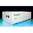
北京欧兰科技发展有限公司为您提供《ITO玻璃中电化学传感器检测方案(激光产品)》,该方案主要用于电子元器件产品中电化学传感器检测,参考标准--,《ITO玻璃中电化学传感器检测方案(激光产品)》用到的仪器有Ekspla NL220型 高能量千赫兹纳秒激光器
相关方案
更多
该厂商其他方案
更多