


方案详情
文
本应用笔记描述了一些在磁性环境下的低温实验,用于开发基于石墨烯的自旋场效应晶体管。使用牛津仪器公司的TeslatronPT Cryofree超导磁体系统和两个专门设计的测量探头进行了测量。
方案详情

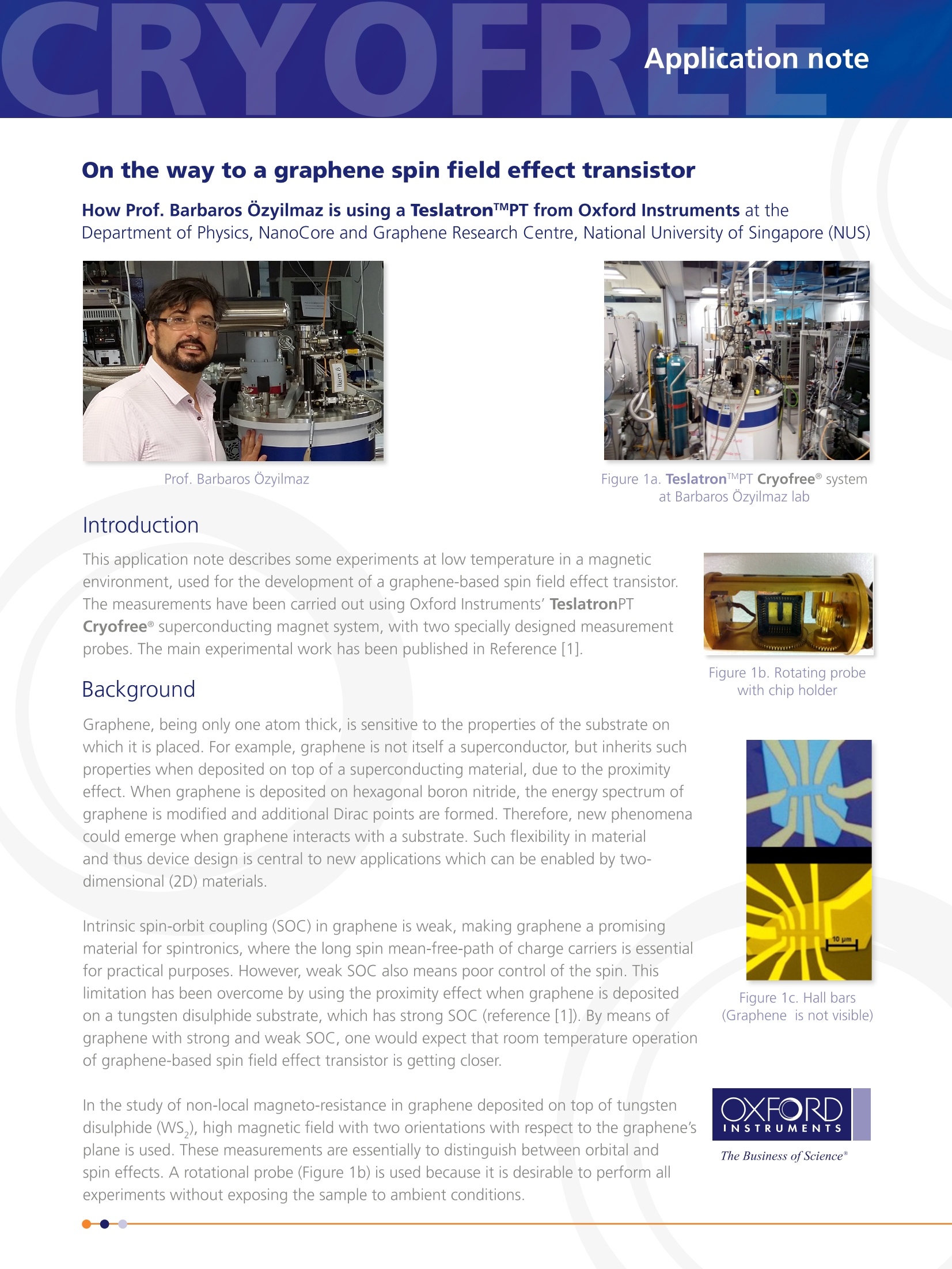
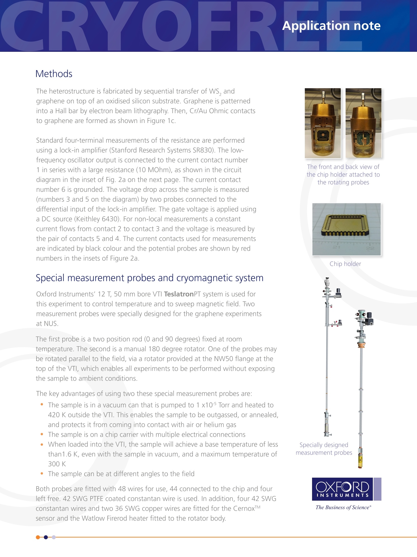
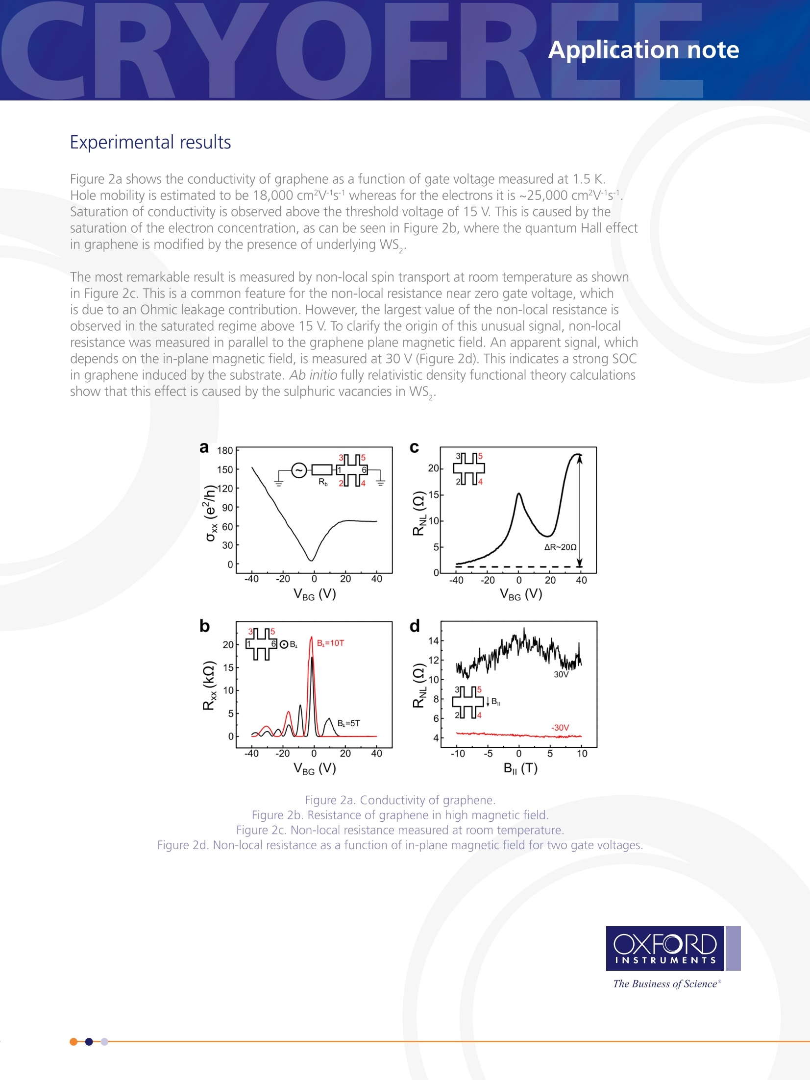
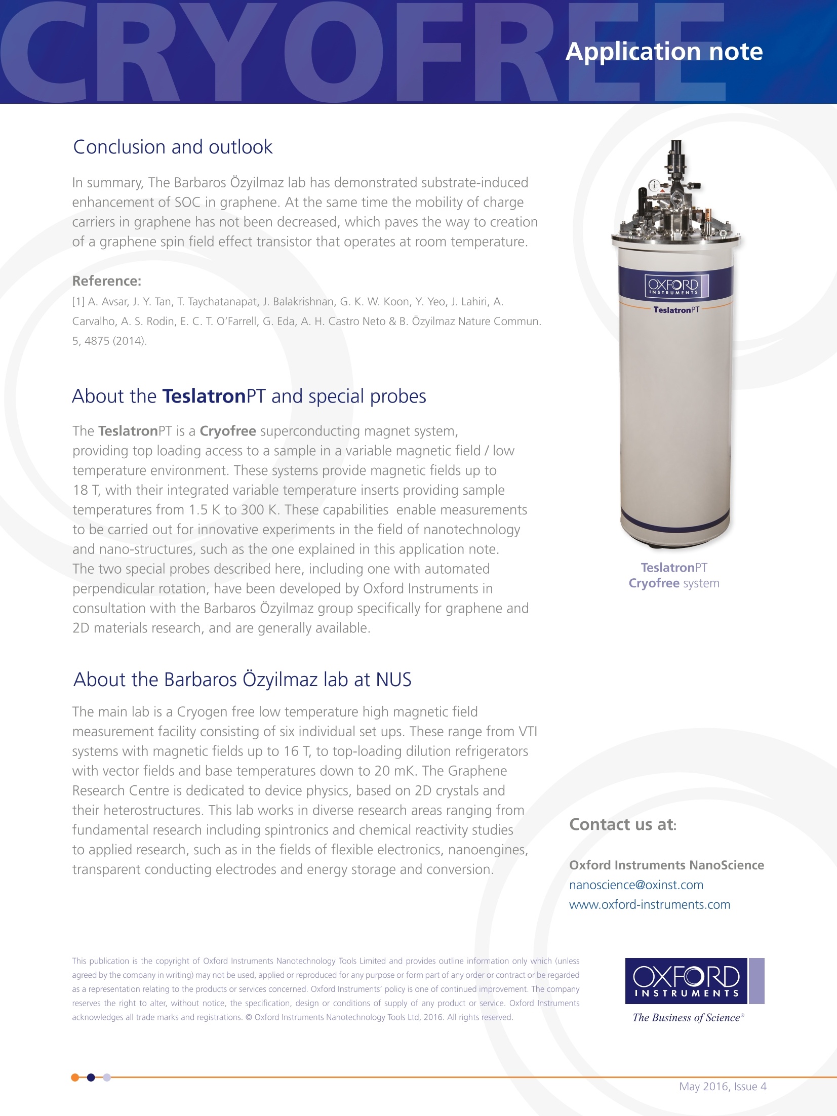
Application note CRYOFFApplication note On the way to a graphene spin field effect transistor How Prof. Barbaros Ozyilmaz is using a TeslatronTMPT from Oxford Instruments at the Department of Physics, NanoCore and Graphene Research Centre, National University of Singapore (NUS) Prof. Barbaros Ozyilmaz Figure 1a. TeslatronTMPT Cryofree@ systemat Barbaros Ozyilmaz lab Introduction This application note describes some experiments at low temperature in a magneticenvironment, used for the development of a graphene-based spin field effect transistor.The measurements have been carried out using Oxford Instruments' TeslatronPTCryofree@ superconducting magnet system, with two specially designed measurementprobes. The main experimental work has been published in Reference [1]. Background Figure 1b. Rotating probewith chip holder Graphene, being only one atom thick, is sensitive to the properties of the substrate onwhich it is placed.For example, graphene is not itself a superconductor, but inherits suchproperties when deposited on top of a superconducting material, due to the proximityeffect. When graphene is deposited on hexagonal boron nitride, the energy spectrum ofgraphene is modified and additional Dirac points are formed. Therefore, new phenomenacould emerge when graphene interacts with a substrate. Such flexibility in materialand thus device design is central to new applications which can be enabled by two-dimensional (2D) materials. Intrinsic spin-orbit coupling (SOC) in graphene is weak, making graphene a promisingmaterial for spintronics, where the long spin mean-free-path of charge carriers is essentialfor practical purposes. However, weak SOC also means poor control of the spin. Thislimitation has been overcome by using the proximity effect when graphene is depositedon a tungsten disulphide substrate, which has strong SOC (reference [1]). By means ofgraphene with strong and weak SOC, one would expect that room temperature operationof graphene-based spin field effect transistor is getting closer. Figure 1c. Hall bars(Graphene is not visible) In the study of non-local magneto-resistance in graphene deposited on top of tungstendisulphide (WS,), high magnetic field with two orientations with respect to the graphene'splane is used. These measurements are essentially to distinguish between orbital andspin effects. A rotational probe (Figure 1b) is used because it is desirable to perform allexperiments without exposing the sample to ambient conditions. The Business ofScience" The heterostructure is fabricated by sequential transfer of WS, andgraphene on top of an oxidised silicon substrate. Graphene is patternedinto a Hall bar by electron beam lithography. Then, Cr/Au Ohmic contactsto graphene are formed as shown in Figure 1c. Standard four-terminal measurements of the resistance are performedusing a lock-in amplifier (Stanford Research Systems SR830). The low-frequency oscillator output is connected to the current contact number1 in series with a large resistance (10 MOhm), as shown in the circuitdiagram in the inset of Fig. 2a on the next page. The current contactnumber 6 is grounded. The voltage drop across the sample is measured(numbers 3 and 5 on the diagram) by two probes connected to thedifferential input of the lock-in amplifier. The gate voltage is applied usinga DC source (Keithley 6430). For non-local measurements a constantcurrent flows from contact 2 to contact 3 and the voltage is measured bythe pair of contacts 5 and 4. The current contacts used for measurementsare indicated by black colour and the potential probes are shown by rednumbers in the insets of Figure 2a. Special measurement probes and cryomagnetic system Oxford Instruments' 12 T, 50 mm bore VTI TeslatronPT system is used forthis experiment to control temperature and to sweep magnetic field.Twomeasurement probes were specially designed for the graphene experimentsat NUS. The first probe is a two position rod (0 and 90 degrees) fixed at roomtemperature. The second is a manual 180 degree rotator. One of the probes maybe rotated parallel to the field, via a rotator provided at the NV50 flange at thetop of the VTI, which enables all experiments to be performed without exposingthe sample to ambient conditions. The key advantages of using two these special measurement probes are: The sample is in a vacuum can that is pumped to 1 x10⁻⁵ Torr and heated to420 K outside the VTI. This enables the sample to be outgassed, or annealed,and protects it from coming into contact with air or helium gas The sample is on a chip carrier with multiple electrical connections When loaded into the VTI, the sample will achieve a base temperature of lessthan1.6 K, even with the sample in vacuum, and a maximum temperature of300K ●The sample can be at different angles to the field Both probes are fitted with 48 wires for use, 44 connected to the chip and fourleft free. 42 SWG PTFE coated constantan wire is used. In addition, four 42 SWGconstantan wires and two 36 SWG copper wires are fitted for the CernoxTMsensor and the Watlow Firerod heater fitted to the rotator body. The front and back view ofthe chip holder attached tothe rotating probes Chip holder 2 Specially designedmeasurement probes The Business ofScience" CRYOFI Experimental results Figure 2a shows the conductivity of graphene as a function of gate voltage measured at 1.5 K.Hole mobility is estimated to be 18,000 cm²V-1s-1 whereas for the electrons it is ~25,000 cm²V-1s-1.Saturation of conductivity is observed above the threshold voltage of 15 V. This is caused by thesaturation of the electron concentration, as can be seen in Figure 2b, where the quantum Hall effectin graphene is modified by the presence of underlying WS,. The most remarkable result is measured by non-local spin transport at room temperature as shownin Figure 2c. This is a common feature for the non-local resistance near zero gate voltage, whichis due to an Ohmic leakage contribution. However, the largest value of the non-local resistance isobserved in the saturated regime above 15 V. To clarify the origin of this unusual signal, non-localresistance was measured in parallel to the graphene plane magnetic field. An apparent signal, whichdepends on the in-plane magnetic field, is measured at 30 V (Figure 2d). This indicates a strong SOCin graphene induced by the substrate. Ab initio fully relativistic density functional theory calculationsshow that this effect is caused by the sulphuric vacancies in WS,. Figure 2a. Conductivity of graphene. Figure 2b. Resistance of graphene in high magnetic field. Figure 2c. Non-local resistance measured at room temperature. Figure 2d. Non-local resistance as a function of in-plane magnetic field for two gate voltages. The Business ofScience" In summary, The Barbaros Ozyilmaz lab has demonstrated substrate-inducedenhancement of SOC in graphene. At the same time the mobility of chargecarriers in graphene has not been decreased, which paves the way to creationof a graphene spin field effect transistor that operates at room temperature. Reference: [1] A. Avsar, J. Y. Tan, T. Taychatanapat, J. Balakrishnan, G. K. W. Koon, Y. Yeo, J. Lahiri, A.Carvalho, A. S. Rodin, E. C. T. O'Farrell, G. Eda, A. H. Castro Neto & B. Ozyilmaz Nature Commun.5,4875 (2014). About the TeslatronPT and special probes The TeslatronPT is a Cryofree superconducting magnet system,providing top loading access to a sample in a variable magnetic field / lowtemperature environment. These systems provide magnetic fields up to18 T, with their integrated variable temperature inserts providing sampletemperatures from 1.5 K to 300 K. These capabilities enable measurementsto be carried out for innovative experiments in the field of nanotechnologyand nano-structures, such as the one explained in this application note.The two special probes described here, including one with automatedperpendicular rotation, have been developed by Oxford Instruments inconsultation with the Barbaros Ozyilmaz group specifically for graphene and2D materials research, and are generally available. About the Barbaros Ozyilmaz lab at NUS The main lab is a Cryogen free low temperature high magnetic fieldmeasurement facility consisting of six individual set ups. These range from VTIsystems with magnetic fields up to 16 T, to top-loading dilution refrigeratorswith vector fields and base temperatures down to 20 mK. The GrapheneResearch Centre is dedicated to device physics, based on 2D crystals andtheir heterostructures. This lab works in diverse research areas ranging fromfundamental research including spintronics and chemical reactivity studiesto applied research, such as in the fields of flexible electronics, nanoengines,transparent conducting electrodes and energy storage and conversion. TeslatronPTCryofree system Contact us at: This publication is the copyright of Oxford Instruments Nanotechnology Tools Limited and provides outline information only which (unlessagreed by the company in writing) may not be used, applied or reproduced for any purpose or form part of any order or contract or be regardedas a representation relating to the products or services concerned. Oxford Instruments' policy is one of continued improvement. The companyreserves the right to alter, without notice, the specification, design or conditions of supply of any product or service. Oxford Instrumentsacknowledges all trade marks and registrations. @ Oxford Instruments Nanotechnology Tools Ltd, 2016. All rights reserved. TeslatronPT是一种Cryofree超导磁体系统,在可变磁场/低温环境中提供样品的顶部加载通道。这些系统提供高达18t的磁场,其集成的可变温度插入片提供从1.5 K到300 K的样品温度。这些能力使测量能够在纳米技术和纳米结构领域进行创新实验,例如本应用说明中解释的实验。这里描述的两种特殊探针,包括一种具有自动垂直旋转的探针,是由牛津仪器公司与Barbaros Özyilmaz团队合作开发的,专门用于石墨烯和2D材料的研究,目前得到普遍应用。
确定
还剩2页未读,是否继续阅读?

产品配置单

牛津仪器科技(上海)有限公司为您提供《石墨烯自旋场效应晶体管中研制方法检测方案(低温恒温器)》,该方案主要用于其他中其它检测,参考标准--,《石墨烯自旋场效应晶体管中研制方法检测方案(低温恒温器)》用到的仪器有 牛津仪器TeslatronPT无液氦磁体低温系统
相关方案
更多
该厂商其他方案
更多