


方案详情
文
本文章介绍了椭圆偏振光谱仪对太阳能薄膜的测量和应用,是了解椭圆偏振光谱仪功能的一篇内容全面的介绍资料。
方案详情

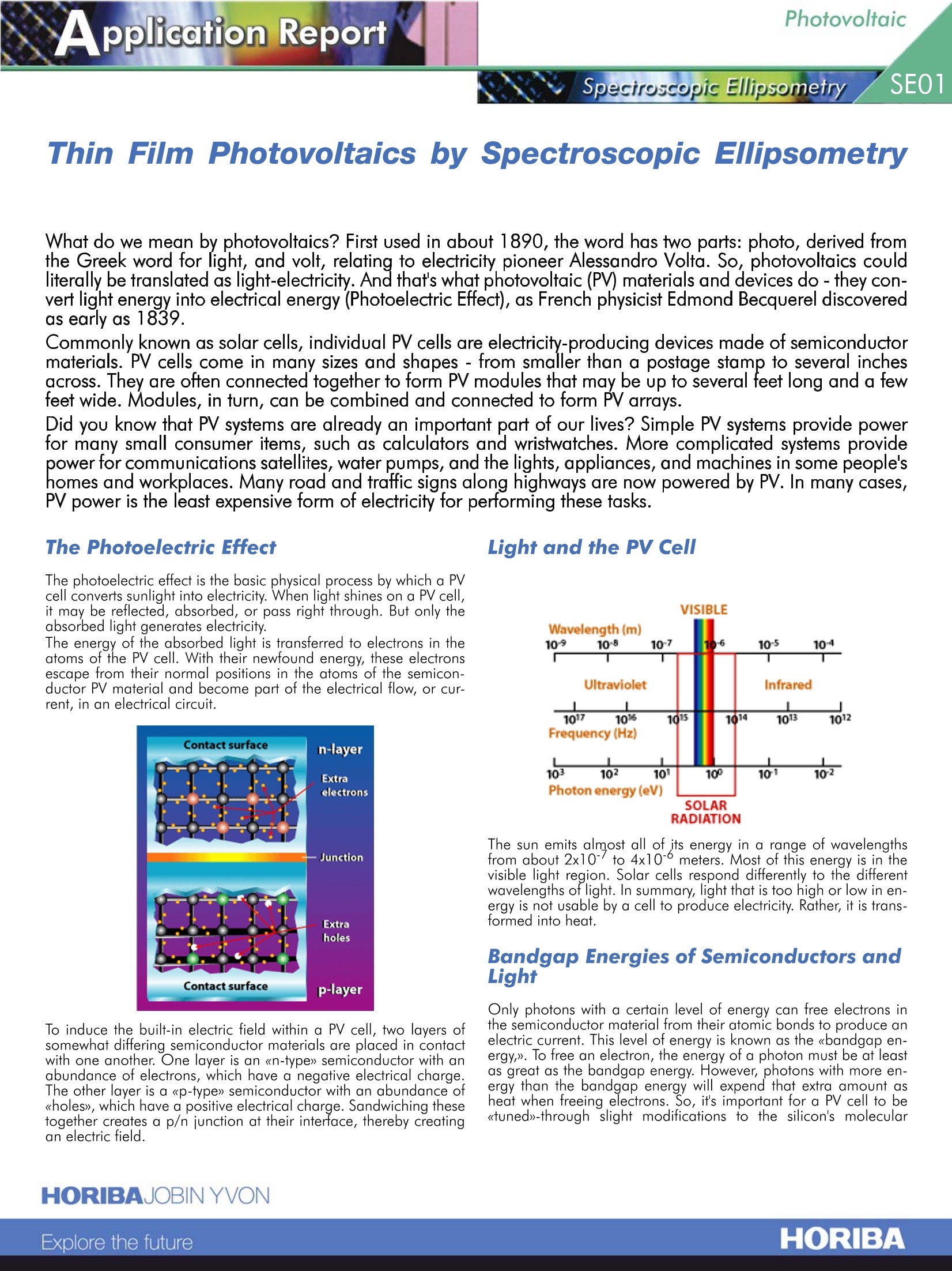
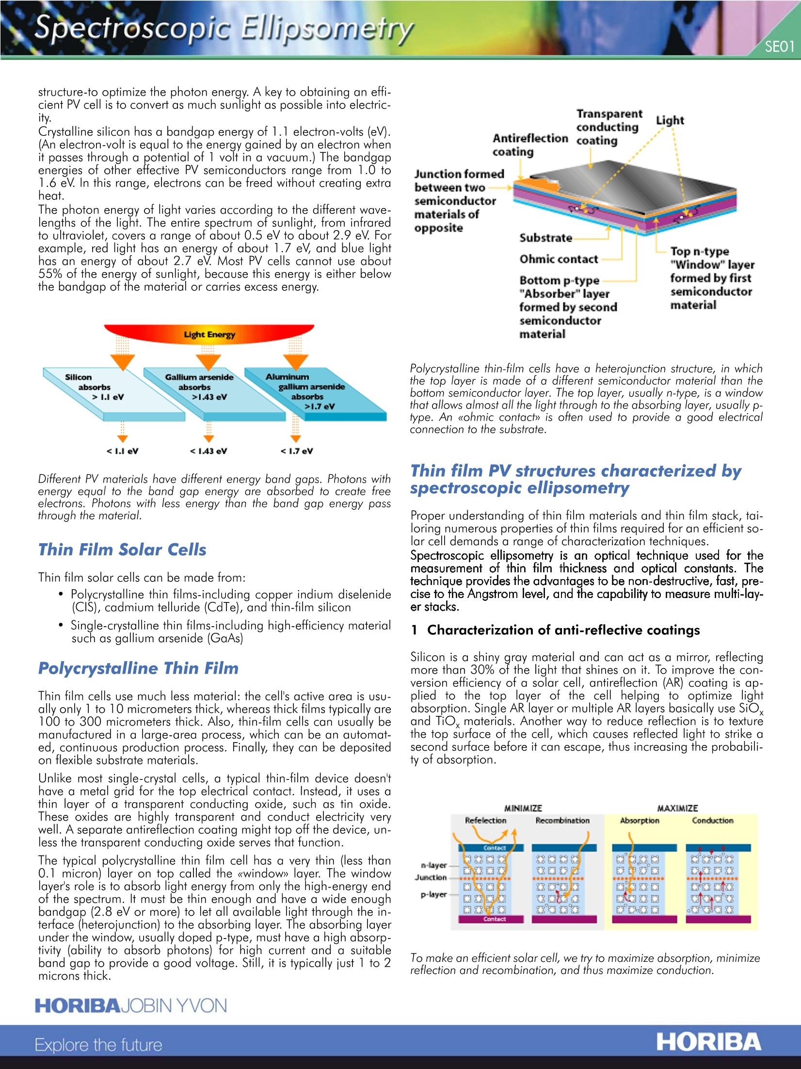
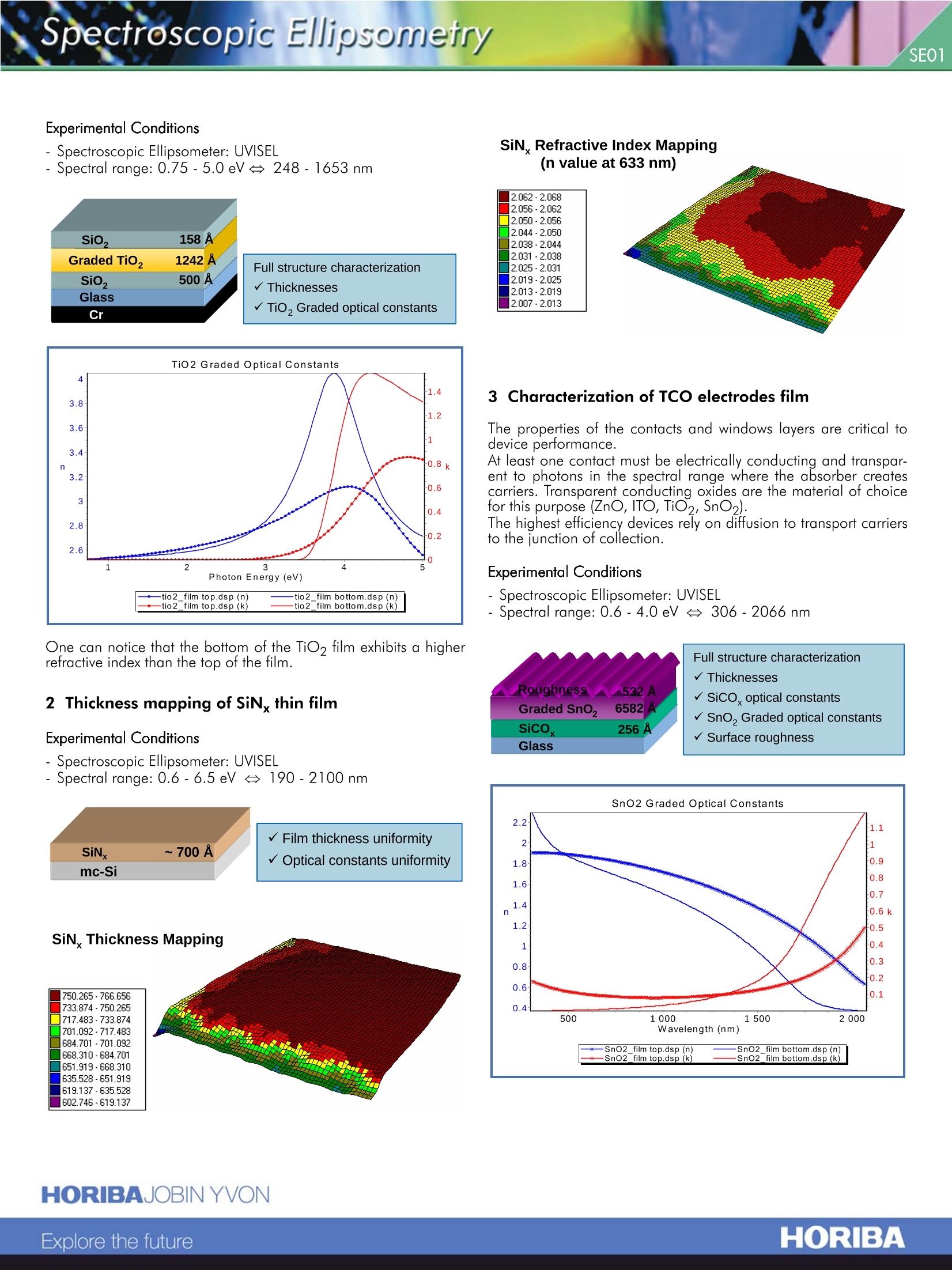
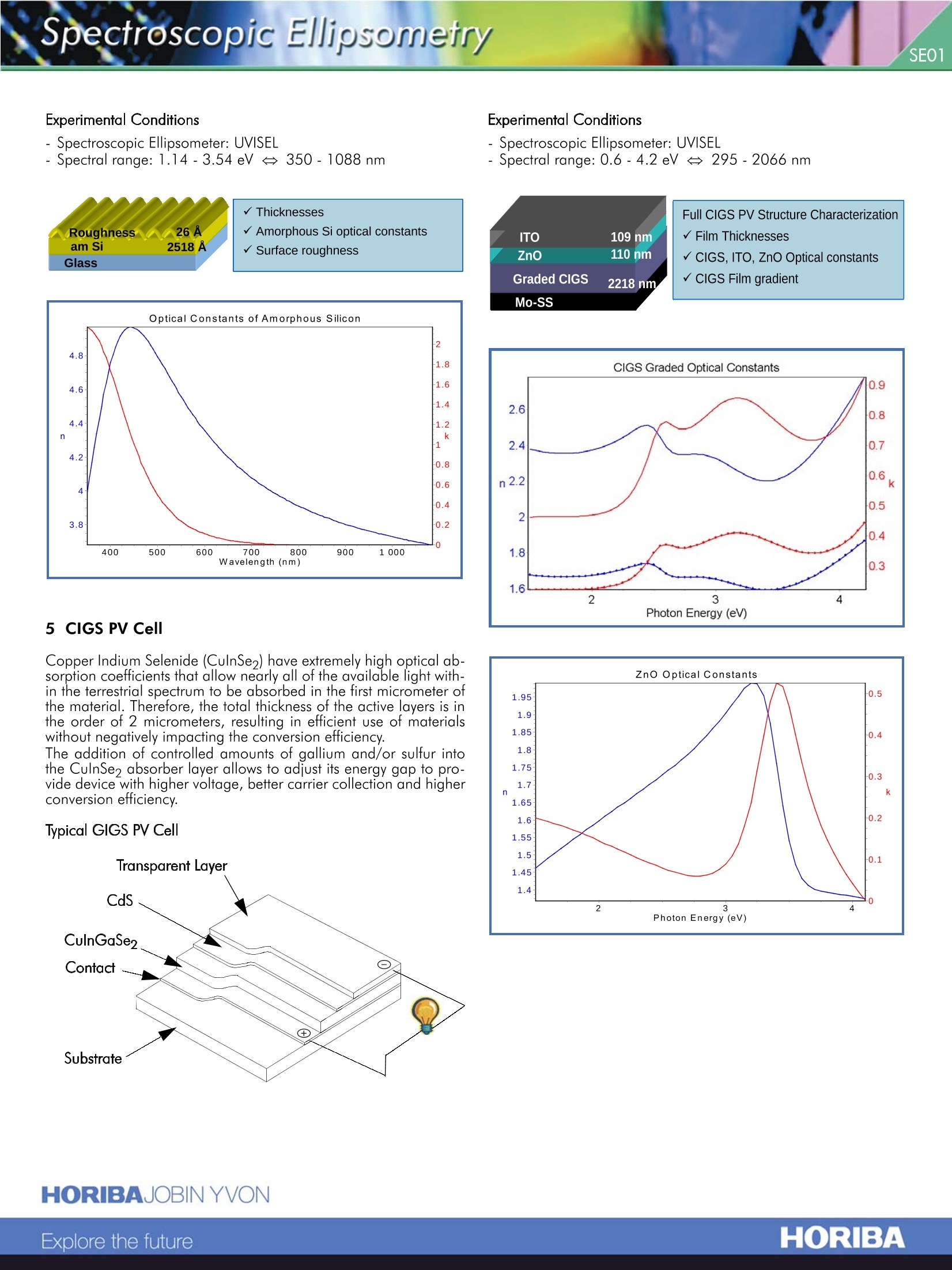
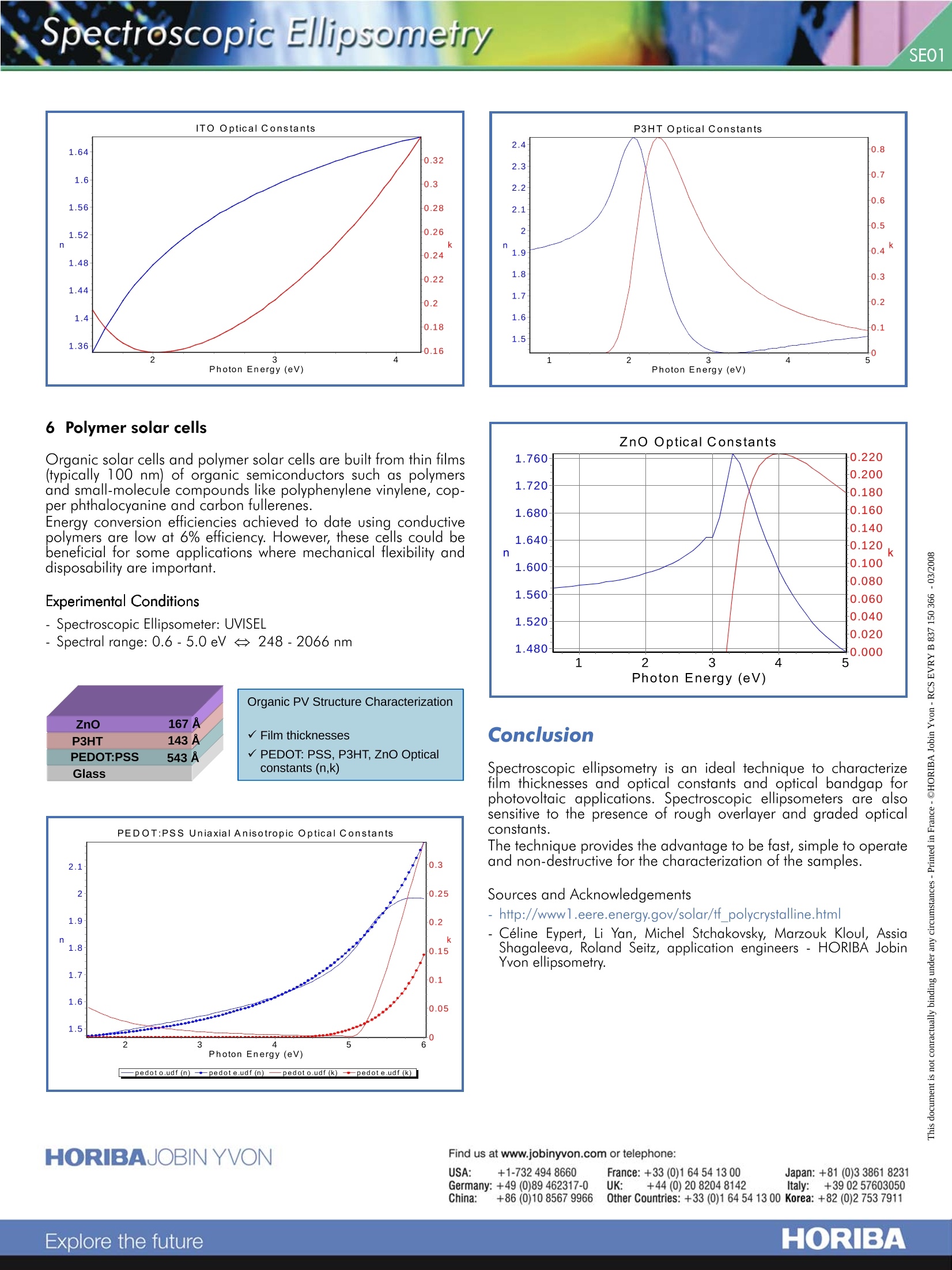
PhotovoltaicArpplication ReportSpectroscopic Ellipsometry Spectroscopic Ellipsometry Thin Film Photovoltaics by Spectroscopic Ellipsometry What do we mean by photovoltaics? First used in about 1890, the word has two parts: photo, derived fromthe Greek word for light, and volt, relating to electricity pioneer Alessandro Volta. So, photovoltaics couldliterally be translated as light-electricity. And that's what photovoltaic (PV) materials and devices do-they con-vert light energy into electrical energy (Photoelectric Effect), as French physicist Edmond Becquerel discoveredas early as 1839 Commonly known as solar cells, individual PV cells are electricity-producing devices made of semiconductorinsmaterials. PV cells come in many sizes and shapes - trom smaller than a postage stamp to several inchesacross. They are often connected together to form PV modules that may be up to several feet long and a fewfeet wide. Modules, in turn, can be combined and connected to form PV arrays. Did you know that PV systems are already an important part of our lives? Simple PV systems provide powerfor many small consumer items, such as calculators and wristwatches. More complicated systems providepower for communications satellites, water pumps, and the lights, appliances, and machines in some people'shomes and workplaces. Many road and traffic signs along highways are now powered by PV. In many cases,PV power is the least expensive form of electricity for performing these tasks. The Photoelectric Effect The photoelectric effect is the basic physical process by which a PVcell converts sunlight into electricity. When light shines on a PV cell,it may be reflected, absorbed, or pass right through. But only theabsorbed light generates electricity. The energy of the absorbed light is transferred to electrons in theatoms of the PV cell. With their newfound energy, these electronsescape from their normal positions in the atoms of the semicon-ductor PV material and become part of the electrical flow, or cur-rent, in an electrical circuit. To induce the built-in electric field within a PV cell, two layers ofsomewhat differing semiconductor materials are placed in contactwith one another. One layer is an《n-type》 semiconductor with anabundance of electrons, which have a negative electrical charge.The other layer is a 《p-type》 semiconductor with an abundance of《holes》, which have a positive electrical charge. Sandwiching thesetogether creates a p/n junction at their interface, thereby creatingan electric field. The sun emits almost all of its energy in a range of wavelengthsfrom about 2x10to 4x10meters. Most of this energy is in thevisible light region. Solar cells respond differently to the differentwavelengths of light. In summary, light that is too high or low in en-ergy is not usable by a cell to produce electricity. Rather, it is trans-formed into heat. Bandgap Energies of Semiconductors andLight Only photons with a certain level of energy can free electrons inthe semiconductor material from their atomic bonds to produce anelectric current. This level of energy is known as the 《bandgap en-ergy》. To free an electron, the energy of a photon must be at leastas great as the bandgap energy. However, photons with more en-ergy than the bandgap energy will expend that extra amount asheat when freeing electrons. So, it’s important for a PV cell to be《tuneds-through slight modifications to the silicon's molecular structure-to optimize the photon energy. A key to obtaining an effi-cient PV cell is to convert as much sunlight as possible into electric-ity. Crystalline silicon has a bandgap energy of 1.1 electron-volts (eV).(An electron-volt is equal to the energy gained by an electron whenit passes through a potential of 1 volt in a vacuum.) The bandgapenergies of other effective PV semiconductors range from 1.0 to1.6 eV. In this range, electrons can be freed without creating extraheat. The photon energy of light varies according to the different wave-lengths of the light. The entire spectrum of sunlight, from infraredto ultraviolet, covers a range of about 0.5 eV to about 2.9 eV. Forexample, red light has an energy of about 1.7 eV, and blue lighthas an energy of about 2.7 eV. Most PV cells cannot use about55% of the energy of sunlight, because this energy is either belowthe bandgap of the material or carries excess energy. Different PV materials have different energy band gaps. Photons withenergy equal to the band gap energy are absorbed to create freeelectrons. Photons with less energy than the band gap energy passthrough the material. Thin Film Solar Cells Thin film solar cells can be made from: ·Polycrystalline thin films-including copper indium diselenide(CIS), cadmium telluride (CdTe), and thin-film silicon ·Single-crystalline thin films-including high-efficiency materialsuch as gallium arsenide (GaAs) Polycrystalline Thin Film Thin film cells use much less material: the cell's active area is usu-ally only 1 to 10 micrometers thick, whereas thick films typically are100 to 300 micrometers thick. Also, thin-film cells can usually bemanufactured in a large-area process, which can be an automat-ed, continuous production process. Finally, they can be depositedon flexible substrate materials. Unlike most single-crystal cells, a typical thin-film device doesn’thave a metal grid for the top electrical contact. Instead, it uses athin layer of a transparent conducting oxide, such as tin oxide.These oxides are highly transparent and conduct electricity verywell. A sepasraatrea taent aintireflection coating might top off the device, un-less the transparent conducting oxide serves that function. The typical polycrystalline thin film cell has a very thin (less than0.1 micron) layer on top called the 《window》 layer. The windowlayer's role is to absorb light energy from only the high-energy endof the spectrum. It must be thin enough and have a wide enoughbandgap (2.8 eV or more) to let all available light through the in-terface (heterojunction) to the absorbing layer. The absorbing layerunder the window, usually doped p-type, must have a high absorp-tivity (ability to absorb photons) for high current and a suitableband gap to provide a good voltage. Still, it is typically just 1 to 2microns thick. Polycrystalline thin-film cells have a heterojunction structure, in whichthe top layer is made of a different semiconductor material than thebottom semiconductor layer. The top layer, usually n-type, is a windowthat allows almost all the light through to the absorbing layer, usually p-type. An 《ohmic contact is often used to provide a good electricalconnection to the substrate. Thin film PV structures characterized byspectroscopic ellipsometry aoper understondiog arttes of thin motericdls ared for an etertlar cell demands a range of characterization techniques.Spectroscopic ellipsometry is an optical technique used for themeasurement of thin film thickness and optical constants. Thetechnique provides the advantages to be non-destructive, fast, pre-cise to the Angstrom level, and the capability to measure multi-lay-er stacks. 1 Characterization of anti-reflective coatings Silicon is a shiny gray material and can act as a mirror, reflectingmore than 30% of the light that shines on it. To improve the con-version efficiency of a solar cell ontireflection (AB) cocting is opabsorption. Single AR layer or multiple AR layers basically use SiO,and TiO, materials. Another way to reduce reflection is to texturethe top surface of the cell, which causes reflected light to strike asecond surface before it can escape, thus increasing the probabili-ty of absorption. To make an efficient solar cell, we try to maximize absorption, minimizereflection and recombination, and thus maximize conduction. Experimental Conditions -Spectroscopic Ellipsometer: UVISEL - Spectral range:0.75-5.0eV<248-1653nm SiO, 158AGraded TiO,2 1242ASio, 500AGlassCr Full structure characterization√Thicknesses√ TiO, Graded optical constants One can notice that the bottom of the TiO2 film exhibits a higherrefractive index than the top of the film. 2 Thickness mapping of SiN, thin film Experimental Conditions -Spectroscopic Ellipsometer: UVISEL - Spectral range: 0.6 -6.5eV 190-2100 nm SiN, Refractive Index Mapping 3 Characterization of TCO electrodes film The properties of the contacts and windows layers are critical todevice performance. At least one contact must be electrically conducting and transpar-ent to photons in the spectral range where the absorber createscarriers. Transparent conducting oxides are the material of choicefor this purpose (ZnO, ITO, TiO2, SnO2). The highest efficiency devices rely on diffusion to transport carriersto the junction of collection. Experimental Conditions Spectroscopic Ellipsometer: UVISEL - Spectral range: 0.6-4.0 eV<306-2066 nm Experimental Conditions - Spectroscopic Ellipsometer: UVISEL - Spectral range: 0.6-6.5eV<190-2100nm Full structure characterization Roughness 27AGraded ZnO900 Ac-Si √Thicknesses√ Graded ZnO optical constants√Surface roughness 4 Characterization of Micro crystalline & AmorphousSilicon thin films Microstructure of silicon films can be varied from one extreme ofamorphous/nanocrystalline to highly oriented and/or epitaxialgrowth. The characterization of silicon thin films by spectroscopic ellipsom-etry provides a wealth of information such as:-Optical bandgap-Inhomogeneities of silicon films (gradient)-The shape of optical constants is directly linked to the microstruc-ture of silicon materials Experimental Conditions · Spectroscopic Ellipsometer: UVISEL - Spectral range: 0.75 -5.0 eV< 248-1653 nm Roughness 83Aum Si 278 Ac-Si √ Thicknesses√Micro crystalline Si optical constants√Surface roughness Experimental Conditions -Spectroscopic Ellipsometer: UVISEL - Spectral range: 0.6-6.5 eV台 190-2100 nm Spectroscopic Ellipsometry Experimental Conditions Experimental Conditions - Spectroscopic Ellipsometer: UVISEL ·Spectroscopic Ellipsometer: UVISEL - Spectral range: 1.14 -3.54 eV<350-1088 nm -Spectral range:0.6-4.2eV295-2066 nm Roughness 26Aam Si 2518AGlass √Thicknesses√ Amorphous Si optical constants√Surface roughness Full CIGS PV Structure Characterization√Film Thicknesses√CIGS, ITO, ZnO Optical constants√CIGS Film gradient 5 CIGS PV Cell Copper Indium Selenide (CulnSe2) have extremely high optical ab-sorption coefficients that allow nearly all of the available light with-in the terrestrial spectrum to be absorbed in the first micrometer ofthe material. Therefore, the total thickness of the active layers is inthe order of 2 micrometers, resulting in efficient use of materialswithout negatively impacting the conversion efficiency. The addition of controlled amounts of gallium and/or sulfur intothe CulnSe absorber layer allows to adjust its energy gap to pro-vide device with higher voltage, better carrier collection and higherconversion efficiency. Typical GIGS PV Cell 6 Polymer solar cells Organic solar cells and polymer solar cells are built from thin films(typically 100 nm) of organic semiconductors such as polymersand small-molecule compounds like polyphenylene vinylene, cop-per phthalocyanine and carbon fullerenes. Energy conversion efficiencies achieved to date using conductivepolymers are low at 6% efficiency. However, these cells could beoeneficial for some applications where mechanical flexibility anddisposability are important. Experimental Conditions · Spectroscopic Ellipsometer: UVISEL . Spectral range: 0.6-5.0eV<248-2066nm Organic PV Structure Characterization √Film thicknesses Conclusion √PEDOT: PSS, P3HT, ZnO Opticalconstants (n,k) Spectroscopic ellipsometry is an ideal technique to characterizefilm thicknesses and optical constants and optical bandgap forphotovoltaic applications. Spectroscopic ellipsometers are alsosensitive to the presence of rough overlayer and graded opticalconstants. The technique provides the advantage to be fast, simple to operateand non-destructive for the characterization of the samples. Sources and Acknowledgements - http://www1.eere.energy.gov/solar/tf_polycrystalline.html - Celine Eypert, Li Yan, Michel Stchakovsky, Marzouk Kloul, AssiaShagaleeva, Roland Seitz, application engineers - HORIBA JobinYvon ellipsometry. HORIBAJOBIN YVON USA: +1-7324948660 France: +33 (0)164541300 Japan:+81 (0)3 3861 8231 China: +86 (0)10 8567 9966 Other Countries: +33 (0)1 64 54 13 00 Korea:+82 (0)2753 7911 HORIBAExplore the future HORIBAExplore the future
确定

还剩4页未读,是否继续阅读?

产品配置单

HORIBA(中国)为您提供《光伏薄膜的椭圆偏振光谱测量》,该方案主要用于薄膜材料中--检测,参考标准--,《光伏薄膜的椭圆偏振光谱测量》用到的仪器有HORIBA Auto SE一键式全自动快速椭偏仪
相关方案
更多
该厂商其他方案
更多