


方案详情
文
本文研究了在镀Mo膜钠钙玻璃(SLG)上共溅射和共蒸发工艺制备的CuIn1-xGaxSe2 (CIGS)吸收膜中主要和次要化学成分的LIBS光谱的影响。结果表明,共溅射技术制备的CIGS层的单脉冲剥烧蚀率高于共蒸发技术制备的CIGS层,从而导致各组分的LIBS信号强度较高。通过对辐照表面形貌和LIBS信号强度变化的研究,发现共溅射技术制备的CIGS薄膜存在元素分馏现象,而共蒸发技术制备的CIGS薄膜没有元素分馏现象。通过x射线衍射检测,证实了两种不同类型CIGS吸收膜的剥蚀和光谱特性的差异是导致其结晶性能差异的原因。此外,LIBS可以有效地测定从SLG扩散而来的CIGS薄膜中钠浓度的深度剖析。
方案详情

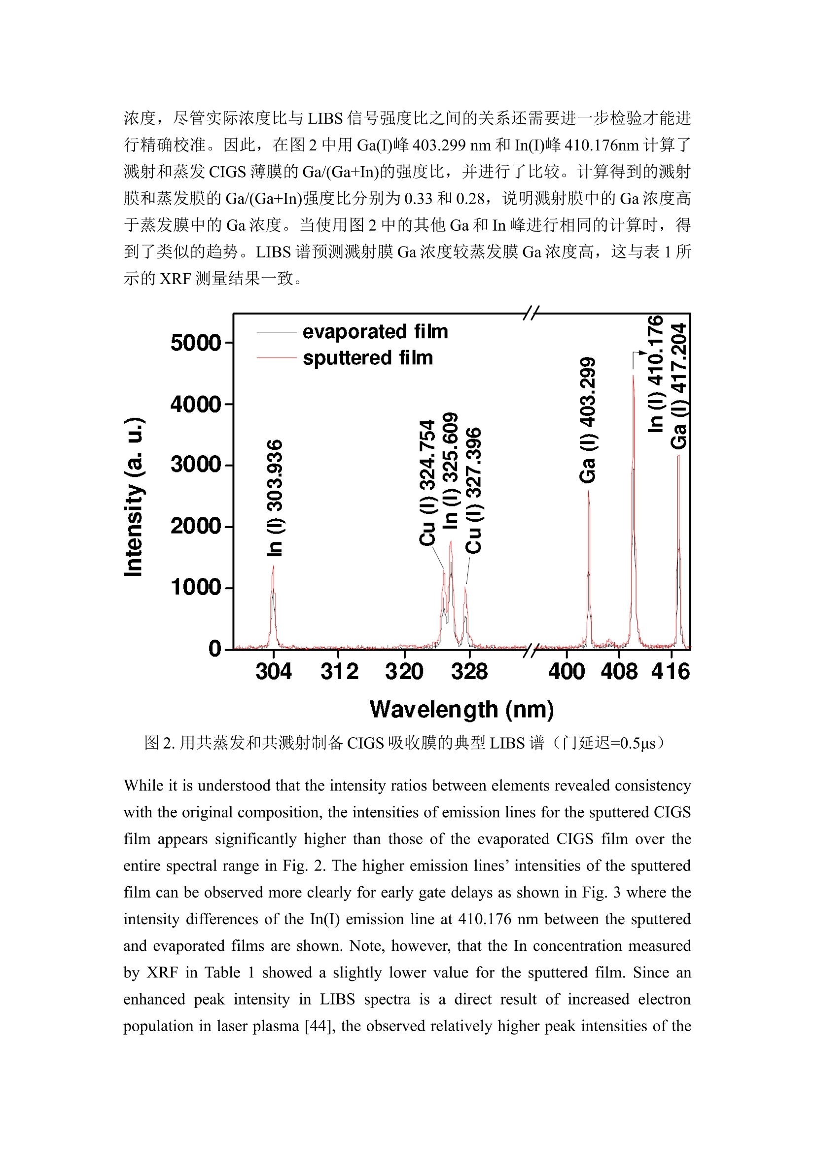
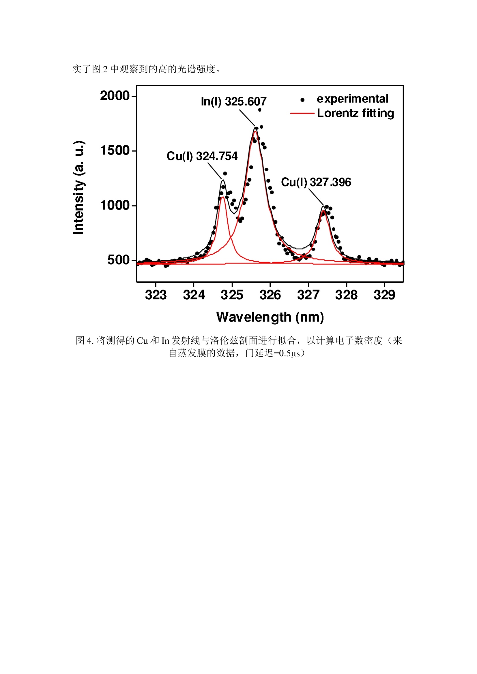
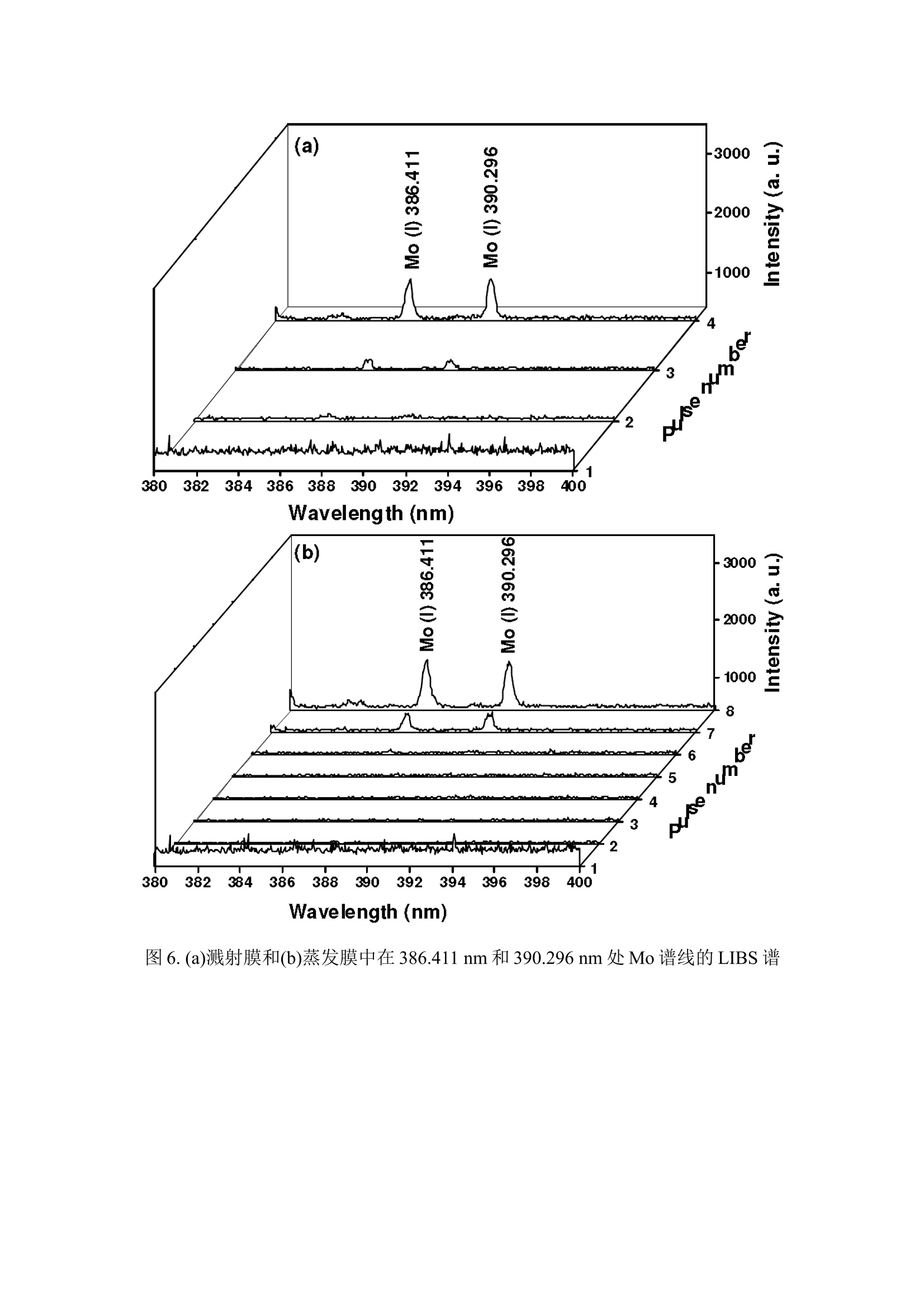
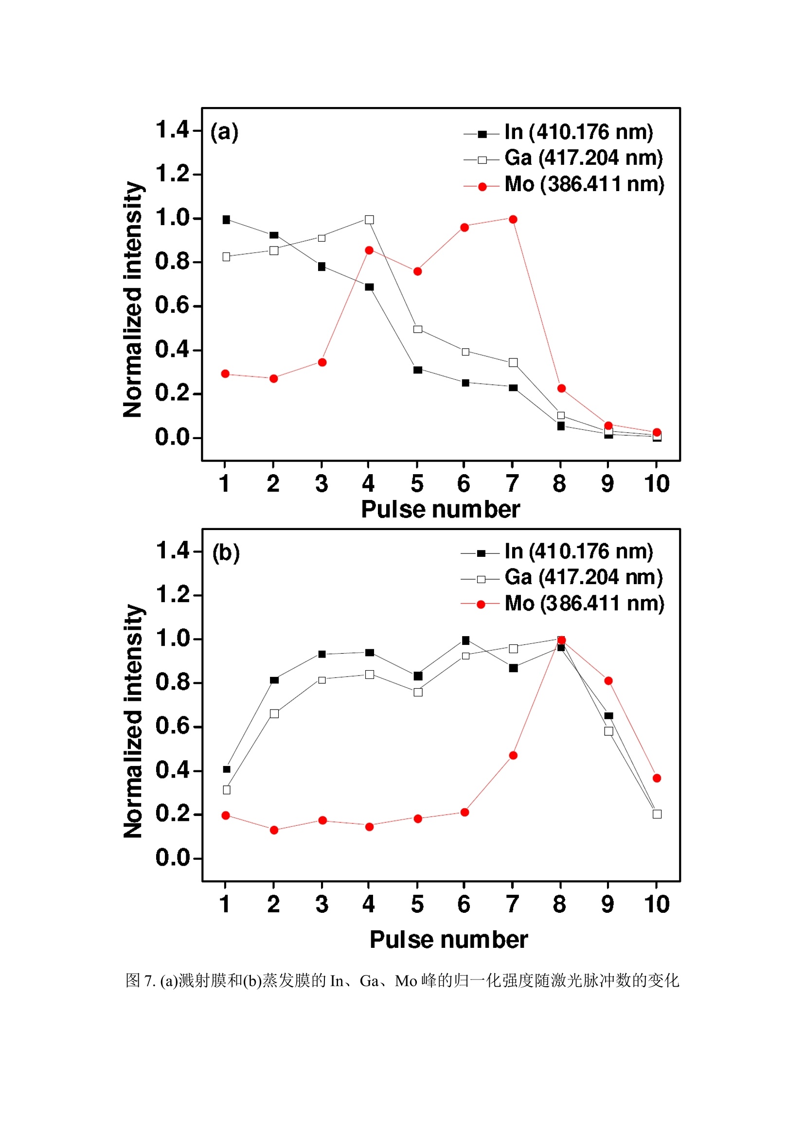
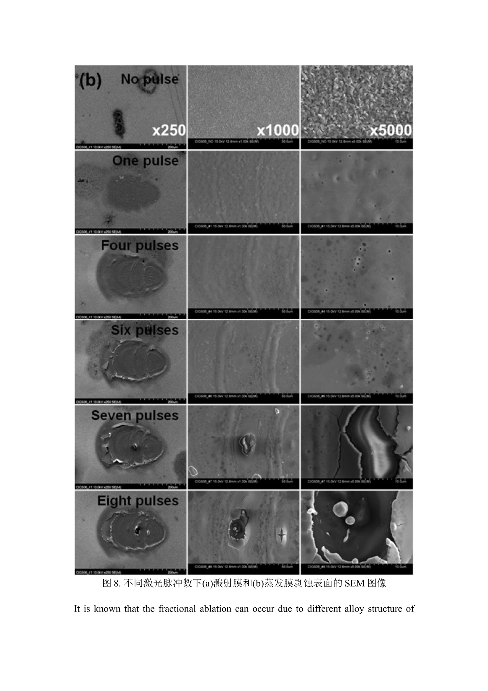
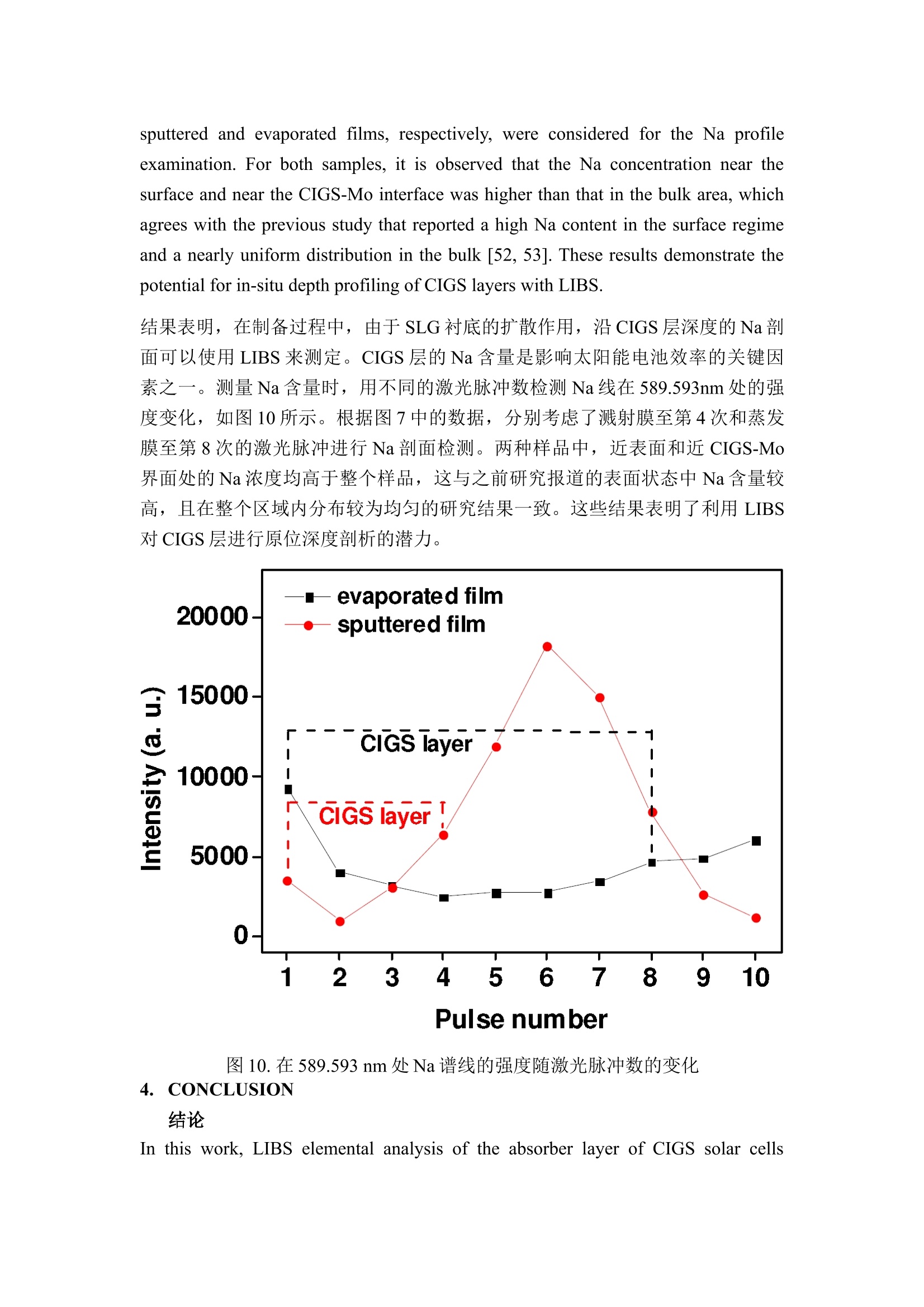
Comparison of the ablation and spectroscopic characteristics of thin CuIn1-xGaxSe2 solar cell films fabricated by coevaporation and co-sputtering processes 共蒸发-共溅射法制备的CuIn1-xGaxSe2太阳能电池薄膜的剥蚀和光谱特征比较 ABSTRACT 摘要 The influence of fabrication processes on the LIBS (Laser Induced Breakdown Spectroscopy) spectra of major and minor chemical constituents in CuIn1-xGaxSe2 (CIGS) absorber films produced by co-sputtering and co-evaporation techniques on Mo-coated soda lime glass (SLG) is reported. It was found that the ablation rate per pulse of CIGS layers fabricated by the cosputtering technique is higher than those fabricated by the co-evaporation technique, resulting in higher LIBS signal intensities of the constituent elements. The examination of surface morphology of irradiated surfaces and changes in LIBS signal intensities revealed evidences of elemental fractionation for the CIGS films fabricated by co-sputtering technique but not for those by co-evaporation technique. From x-ray diffraction measurements, it was confirmed that the differences in the ablation and spectroscopic characteristics of the two different types of CIGS absorber films were contributed to the differences in crystalline properties. Furthermore, it was demonstrated that LIBS can effectively determine a depth profile of sodium concentration in CIGS thin films, diffused from SLG. 本文研究了在镀Mo膜钠钙玻璃(SLG)上共溅射和共蒸发工艺制备的CuIn1-xGaxSe2 (CIGS)吸收膜中主要和次要化学成分的LIBS光谱的影响。结果表明,共溅射技术制备的CIGS层的单脉冲剥烧蚀率高于共蒸发技术制备的CIGS层,从而导致各组分的LIBS信号强度较高。通过对辐照表面形貌和LIBS信号强度变化的研究,发现共溅射技术制备的CIGS薄膜存在元素分馏现象,而共蒸发技术制备的CIGS薄膜没有元素分馏现象。通过x射线衍射检测,证实了两种不同类型CIGS吸收膜的剥蚀和光谱特性的差异是导致其结晶性能差异的原因。此外,LIBS可以有效地测定从SLG扩散而来的CIGS薄膜中钠浓度的深度剖析。 INTRODUCTION 引言 The second generation solar cells based on thin absorber layers such as amorphous silicon (a-Si), CdTe, or CuIn1-xGaxSe2 (CIGS) have several advantages as compared to the first generation solar cells based on crystalline silicon (c-Si). For example, thin film solar cells can be manufactured at a lower cost than the c-Si counterparts [1]. Also, due to manufacturability on flexible substrates, thin film solar cells can be easily integrated into the roof or exterior walls of a building [2]. Accordingly, there have been tremendous research efforts to enhance the photoconversion efficiency of thin film solar cells and to develop cost-effective manufacturing technologies. Among the various types of thin film solar cells, CIGS solar cells offer several attractive properties for practical solar power applications such as high absorption coefficient and high photo-conversion efficiency of greater than 20% [3, 4]. The high absorption coefficient of CIGS absorbing layer allows the effective film thickness to be in the range of only 1 ~ 2 microns, greatly reducing the material usage and associated costs compared to c-Si solar cells. 第二代太阳能电池基于薄吸收膜如非晶硅(a-Si),碲化镉(CdTe),或CuIn1-xGaxSe2 (CIGS),相比于第一代太阳能电池基于晶体硅(c-Si)有几个优势。例如,薄膜太阳能电池的制造成本比c-Si的[1]要低。此外,由于薄膜太阳能电池可在柔性基板上制造,因此可以很容易集成到建筑物的屋顶或外墙上。因此,为了提高薄膜太阳能电池的光电转换效率和开发具有成本效益的制造技术,人们进行了大量的研究工作。在各种类型的薄膜太阳能电池中,CIGS太阳能电池具有吸收系数高、光能转换效率大于20%的优点[3,4], 在实际太阳能应用中具有很大的吸引力。CIGS吸收层的高吸收系数使得有效薄膜厚度在1 ~ 2微米范围内,与c-Si太阳能电池相比,大大降低了材料的使用量和相关成本。 The fabrication of thin CIGS absorbing layer can be achieved by various methods that include sputtering [5-8], co-evaporation [9-11], electrodeposition [12], spray pyrolysis [13], paste coating [14] etc. Among these techniques, co-evaporation (shortly, evaporation) and cosputtering (shortly, sputtering) processes are the preferred methods for commercial manufacturing due to process scalability to mass production with consistent and high photoconversion efficiency performance. In the evaporation process, the constituent elements (Cu, In, Ga, and Se) are simultaneously vaporized in a chamber and homogeneous CIGS thin film is then formed by surface reaction on a substrate. The highest cell efficiency of 20.3 % has been recorded from the thin absorber film obtained by three-stage evaporation method [3]. In a twostep sputtering process, the Cu-In-Ga precursor thin films are deposited on the substrate from the metal targets of Cu, In, Ga or their alloys such as CuGa, CuIn, and In2Se3, and the CIGS films are obtained by subsequent reaction with selenium source in the elevated temperature environment. The sputtering-based processes could be more adaptable for large area and continuous fabrication due to its simpler fabrication steps and the availability of existing manufacturing facilities. 通过溅射[5-8]、共蒸发[9-11]、电沉积[12]、喷涂热解[13]、涂覆法[14]等多种方法制备薄CIGS吸收层。在这些技术中,共蒸发和共溅射工艺是商用制造的首选方法,由于工艺的可扩展性,大规模生产具有一致和高的光转换效率性能。蒸发过程中,Cu、In、Ga、Se等组成元素在样品室内同时汽化,然后在衬底上通过表面反应形成均匀的CIGS薄膜。采用三步蒸发法制得的薄膜的电池效率最高,达到20.3%。在两步溅射过程中,Cu-In-Ga预置层是由Cu、In、Ga或其合金(如CuGa、CuIn、In2Se3)的金属靶沉积在衬底上,CIGS薄膜是在高温环境下与硒源进行后续反应得到的。基于溅射的工艺由于其简单的制造步骤和现有制造设备的可用性,更适合于大面积的连续制造。 Although many factors are known to influence on the efficiency of CIGS solar cell devices, the primary factor that requires most rigorous control is the elemental composition of the CIGS absorber layer. The stoichiometric ratio of main chemical constituents of the CIGS absorber is known to govern its energetic and electronic properties [15-18]. Therefore, an accurate measurement of the elemental composition of CIGS absorber layer is a crucial and challenging issue for the fabrication process development and manufacturing of high efficiency CIGS solar cells. Several analytical methods such as secondary ion mass spectrometry (SIMS) [19], inductively coupled plasma optical emission spectroscopy (ICP-OES) [20], glow discharge mass spectrometry (GDMS) [21], laser induced breakdown spectroscopy (LIBS) [22-23], or xray fluorescence (XRF) [3] have been applied for the elemental analysis of solar cells. Among these methods, however, only LIBS and XRF measurements can be performed under atmospheric environment without the need for complex vacuum systems, thereby allowing insitu monitoring and thus quality control compositional measurements during CIGS films manufacturing. More commonly accepted technique such as ICP-OES requires extensive sample preparation involving acid dissolution of bulk samples and the measurement takes too long for it to be an effective in-line method for production control. 虽然影响CIGS太阳能电池器件效率的因素很多,但最需要严格控制的主要因素是CIGS吸收薄膜的元素组成。CIGS吸收薄膜的主要化学成分的化学计量比是已知控制其能量和电子性能的关键[15-18]。因此,准确测量CIGS吸收薄膜的元素组成,是高效CIGS太阳能电池制造工艺的发展和制造面临的关键和挑战。二次离子质谱(SIMS)[19]、电感耦合等离子体发射光谱(ICP-OES)[20]、辉光放电质谱(GDMS)[21]、激光诱导击穿光谱(LIBS)[22-23]或x射线荧光(XRF)[3]等分析方法已被应用于太阳能电池的元素分析。然而,在这些方法中,只有LIBS和XRF测量可以在大气环境下进行,而不需要复杂的真空系统,从而允许在CIGS薄膜制造过程中进行现场监测,从而进行质量控制、成分测量。比较普遍接受的技术,如ICP-OES,需要大量的样品制备,包括大体积样品的酸溶,测量时间太长,不能作为一种有效的在线生产控制方法。 LIBS is a powerful method for elemental analysis in which real-time analysis, high sensitivity, and no sample preparation [24-32] are desired. LIBS has been successfully applied for environmental monitoring [33-35], biological species detection [36], military applications [37], precious artworks analysis [38], nuclear power station inspection [39], depth profiling of thin film materials [40,41], etc. Recently, Darwiche et al. [22] reported the multi-elemental analytical characterization of different qualities of solid silicon using LIBS, in particular, the investigation of optimal environmental parameters such as the pressure and the composition of buffering gas to improve detection limit of impurities such as boron, calcium and chromium etc. and addressed the application of LIBS for solar cell industry. Since LIBS only requires nano to micro grams of mass for effective analysis, a thin film of 100 nm in thickness or less can be analyzed by LIBS for elemental composition [41]. Consequently, LIBS could be the most effective technique for high-resolution elemental mapping and depth profiling analyses of thin CIGS layers. Furthermore, sodium (Na), one of the key elements governing the efficiency of CIGS solar cells, can be measured with high detection sensitivity down to ppm level using LIBS. This provides LIBS a distinct advantage over XRF due to the XRF technique’s ineffectiveness for lighter elements including Na. The short analysis time of LIBS, one second or less per single laser shot measurement [42], is another strong advantage for enabling rapid compositional characterization and implementing real-time quality control in manufacturing lines. Despite these clear advantages of LIBS, the applications of LIBS for elemental analysis of thin film solar cell materials has been hardly investigated and very limited number of research papers [43] have been published for LIBS analysis of CIGS absorber layer up to date. LIBS是一种功能强大的元素分析方法,实时分析,灵敏度高,不需要样品制备[24-32]。LIBS已成功应用于环境监测[33-35]、生物物种检测[36]、军事应用[37]、珍贵艺术品分析[38]、核电站检测[39]、薄膜材料深度剖析等[40,41]。最近,Darwiche等人[22]研究使用LIBS对不同质量的固体硅进行多元素分析表征,特别是研究了缓冲气体的压力、组成等最佳环境参数,提高了硼、钙、铬等杂质的检出限,并探讨了LIBS在太阳能电池工业中的应用。LIBS只需要纳克到微克的质量就可以进行有效的分析,因此可以用LIBS分析100 nm或更小厚度的薄膜,得到元素组成[41]。因此,LIBS可能是对CIGS薄膜进行高分辨率元素分布和深度剖析的最有效技术。此外,钠(Na)是控制CIGS太阳能电池效率的关键元素之一,可以使用LIBS以高检测灵敏度测量到ppm水平。这使得LIBS比XRF具有明显的优势,因为XRF技术无法检测包括Na在内的较轻元素。LIBS的分析时间短,每次激光测量的时间不超过1秒[42],这是在生产线上实现快速成分表征和实时质量控制的另一个强大优势。尽管LIBS具有这些明显的优点,但是LIBS在薄膜太阳能电池材料元素分析中的应用还很少被研究,目前发表LIBS分析CIGS吸收薄膜方面的研究论文非常有限。 In this work, we report the results for LIBS analyses of CIGS thin absorber films fabricated by sputtering- and evaporation-based processes. The differences in ablation characteristics and LIBS signal intensity of the CIGS layers fabricated by these two different deposition methods were compared. In addition, their microstructural properties were investigated by x-ray diffraction (XRD) and scanning electron microscopy (SEM). It is shown that the observed differences between the sputtered and evaporated films are associated with microstructural properties of the CIGS films. 在这项工作中,我们报告了用溅射和蒸发法制备的CIGS薄膜的LIBS分析结果。比较了两种不同沉积方法制备的CIGS层的剥蚀特性和LIBS信号强度的差异。此外,还通过x射线衍射(XRD)和扫描电镜(SEM)对其微观结构进行了研究。结果表明,溅射膜和蒸发膜之间的差异与CIGS薄膜的微观结构有关。 EXPERIMENTAL SETUP 实验装置 The polycrystalline CIGS absorber films were grown by either a three-stage evaporation process or a two-step sputtering process as illustrated in Fig. 1. For substrate, soda-lime glass (SLG) (Abrisa Co.) coated with a Mo layer of below 1 μm thickness was utilized. The Mo layer functions as the back electrode of a solar cell. For the fabrication of evaporated films, In, Ga and Se sources were first simultaneously evaporated at the substrate temperature of 400℃ to form a (In,Ga)2Se3 layer with a thickness of 1 μm, then as the second step Cu and Se were evaporated and reacted with the (In,Ga)2Se3 layer at the substrate temperature of 600 °C to form a Cu-rich phase, and finally In, Ga and Se elements were again evaporated maintaining the same substrate temperature to produce a Cu-poor phase. For the sputtered films, a Cu-In-Ga precursor film was first fabricated with the thickness of ca. 0.8 μm by simultaneous sputtering of Cu0.6Ga0.4 and Cu0.5In0.5 targets, and then the CIGS film was obtained by subsequent selenization reaction between precursor film and the Se source provided from a downstream Se cracker (JMON, Korea) at the substrate temperature of 550 ℃ for 80 min. 用三步蒸发法或两步溅射法制备了多晶CIGS吸收膜,如图1所示。 图1 说明了采用(a)共蒸发工艺和(b) 共溅射工艺过程 衬底:涂有小于1μm厚度的Mo涂层的钠钙玻璃(SLG) (Abrisa有限公司)。Mo层作为太阳能电池的背电极。制作蒸发薄膜,在400℃衬底温度下,首先同时蒸发In、Ga和Se源,形成1μm厚的(In,Ga)2Se3层。第二步在600℃的衬底温度下,蒸发Cu和Se,与(In,Ga)2Se3层反应形成富Cu相。最后,保持相同的衬底温度,In、Ga和Se元素再次蒸发,产生贫铜相。对于溅射的薄膜,通过同时溅射Cu0.6Ga0.4 and Cu0.5In0.5靶首先制作出约0.8μm厚的Cu-In-Ga预置层。然后在550℃的衬底温度下,预置层与Se源(JMON, Korea)进行80min硒化反应得到CIGS薄膜。 The differences in crystallographic characteristics of the CIGS thin films prepared by both methods were investigated by XRD measurements (Rigaku X-ray diffractormeter with Cu Kα radiation). The chemical composition and thickness of both CIGS thin films were measured by XRF using the CIGS calibration sample consisting of 18.4 at% Cu, 14.3 at% In, 5.0 at% Ga and 62.3 at% Se with the thickness of 2.15 μm (F12H28F11-2, Calmetrics Inc.) as the reference, and the results are summarized in Table 1. The CIGS films appeared to have the same thickness but different compositions. The evaporated film was found to be a Cu-poor film (CuIn1.1Ga0.19Se2.32), whereas the sputtered film resulted in a Se-poor phase (CuIn0.75Ga0.25Se1.53). 通过XRD (Rigaku X-ray diffractormeter with Cu Kα radiation)测试,研究了两种方法制备的CIGS薄膜的晶体特性的差异。用XRF法测定了两种CIGS薄膜的化学成分和厚度,使用厚2.15μm含18.4% Cu、14.3 % In、5.0 % Ga和 62.3 % Se的CIGS校准样品(F12H28F11-2, Calmetrics Inc.)作为参照,结果如表1所示。 表1 用XRF检测了共蒸发和共溅射工艺制备的CIGS吸收膜的组成和厚度 制备方法 厚度(μm) 组成(%) 元素比例 CIGS Mo Cu In Ga Se [Ga]/[ Ga+ In] 溅射 1.23 0.57 28.19 21.63 7.28 43.17 0.25 蒸发 1.23 0.76 21.63 23.83 4.15 50.39 0.15 CIGS膜的厚度相同,但组成不同。蒸发制备的薄膜被发现是贫铜薄膜(CuIn1.1Ga0.19Se2.32),溅射制备的薄膜是贫硒薄膜(CuIn0.75Ga0.25Se1.53)。 LIBS analyses of the two CIGS absorber films were carried out by using a commercial LIBS system (Applied Spectra Inc., Model: RT100-HP). The measurement system was equipped with a high performance Czerny-Turner spectrometer that had a dual-grating turret providing maximum spectral resolution of 0.1 nm with a 40 nm spectral window. A Q-switched Nd:YAG laser (λ=1064 nm, τ=4ns) with a near top-hat spatial profile was used to generate plasma with a fixed spot diameter of 150 μm. 利用商用LIBS系统(Applied Spectra Inc., Model: RT100-HP)对两种CIGS吸收膜进行了LIBS分析。该测量系统配备了一台高性能的Czerny-Turner光谱仪,该光谱仪有一个双光栅转台,提供了0.1 nm的最大光谱分辨率和40 nm的光谱窗口。Q开关Nd: YAG激光器(λ= 1064 nm,τ= 4 ns),拥有近乎高帽光束轮廓的激光,用于生成150μm固定光斑直径的等离子体。 For LIBS measurement, ten laser pulses were successively shot on the same spot of each sample at the rate of 1 Hz and the evolution of LIBS spectra with respect to pulse number was examined. SEM (Hitach S-4700) images of the ablated surfaces at different pulse numbers were taken to check the changes in surface morphology. 在LIBS检测中,以1hz的频率在每个样品的同一点连续发射10个激光脉冲,观察LIBS光谱随脉冲数的变化。采用SEM (Hitach S-4700)对不同脉冲数的烧蚀表面进行扫描,检测表面形貌的变化。 RESULTS AND DISCUSSION 结果与讨论 Fig. 2 shows the typical LIBS spectra of the two types of CIGS sample over the spectral ranges of 298-338 and 395-418 nm, separated by a break line. The laser energy used for these measurements was 0.48 mJ, corresponding to laser fluence of 2.72 J/cm2, and the gate delay was 0.5 μs. These values of laser pulse energy and gate delay yielded the maximum signal to background ratio (SBR) and minimum full width at half maximum (FWHM) of the LIBS emission lines of analyzed chemical constituents. In general, the emission peak intensities of the constituent elements reflect the original concentration of those elements within the target, although the relation between the ratio of actual concentration and the ratio of LIBS signal intensities needs to be further examined for precise calibration. Thus, the intensity ratios of Ga/(Ga+In) for both sputtered and evaporated CIGS films were calculated with Ga(I) peak at 403.299 nm and In(I) peak at 410.176nm in Fig. 2 and compared. The calculated Ga/(Ga+In) intensity ratios of the sputtered and evaporated films were 0.33 and 0.28, respectively, implying that Ga concentration in the sputtered film is higher than that in the evaporated film. Similar trends were obtained when other Ga and In peaks in Fig. 2 were used for the same calculation. The relatively higher Ga concentration of the sputtered film than that of the evaporated film predicted by these LIBS spectra agrees with the XRF measurement results shown in Table 1. 图2显示了两种CIGS样品在298-338nm和395-418 nm光谱范围内的典型LIBS光谱,中间用一条折线隔开。用于这些检测的激光能量为0.48 mJ,对应的激光能量密度为2.72 J / cm2,0.5μs门延迟。这些激光脉冲能量和门延迟的值产生了分析化学成分的LIBS发射谱线的最大信号背景比(SBR)和最小半峰宽(FWHM)。一般来说,组成元素的发射峰强度反映了这些元素在样品内的原始浓度,尽管实际浓度比与LIBS信号强度比之间的关系还需要进一步检验才能进行精确校准。因此,在图2中用Ga(I)峰403.299 nm和In(I)峰410.176nm计算了溅射和蒸发CIGS薄膜的Ga/(Ga+In)的强度比,并进行了比较。计算得到的溅射膜和蒸发膜的Ga/(Ga+In)强度比分别为0.33和0.28,说明溅射膜中的Ga浓度高于蒸发膜中的Ga浓度。当使用图2中的其他Ga和In峰进行相同的计算时,得到了类似的趋势。LIBS谱预测溅射膜Ga浓度较蒸发膜Ga浓度高,这与表1所示的XRF测量结果一致。 图2. 用共蒸发和共溅射制备CIGS吸收膜的典型LIBS谱(门延迟=0.5μs) While it is understood that the intensity ratios between elements revealed consistency with the original composition, the intensities of emission lines for the sputtered CIGS film appears significantly higher than those of the evaporated CIGS film over the entire spectral range in Fig. 2. The higher emission lines’ intensities of the sputtered film can be observed more clearly for early gate delays as shown in Fig. 3 where the intensity differences of the In(I) emission line at 410.176 nm between the sputtered and evaporated films are shown. Note, however, that the In concentration measured by XRF in Table 1 showed a slightly lower value for the sputtered film. Since an enhanced peak intensity in LIBS spectra is a direct result of increased electron population in laser plasma [44], the observed relatively higher peak intensities of the sputtered film is considered to imply that a higher electron population was attained within the sputtered-film laser plasma. It is assumed that since both films were made of the same constituting elements, there exist no fundamental differences in the emission transition characteristics of those elements in both films. 虽然我们知道元素之间的强度比与原始成分一致,但在图2中,在整个光谱范围内,溅射CIGS薄膜的发射谱线强度明显高于蒸发CIGS薄膜的发射谱线强度。在图3中,溅射膜和蒸发膜在410.176 nm处的In (I)发射线的强度差异,可以更清晰地观察到溅射膜的高发射线强度。但是,请注意,表1中XRF测量的In浓度值显示溅射膜的值略低。由于激光等离子体[44]中电子密度的增加直接导致了LIBS谱中电子密度的增强,因此溅射膜中所观察到的相对较高的峰值强度意味着溅射膜激光等离子体具有更高的电子密度。假设这两种薄膜都是由相同的构成元素构成,所以这两种薄膜中这些元素的发射跃迁特性不存在根本差异。 图3. 两种CIGS薄膜在410.176 nm处的In(I)发射线的强度随门延迟的变化。 From the measured LIBS spectra, the electron number density of laser plasmas produced from the sputtered and evaporated films can be estimated as follows. First, it was assumed that the FWHM of the measured intensity peaks was determined mainly by the Stark effect and instrumental characteristics. Then, the electron density could be found from the following relation [45], 根据测得的LIBS谱,溅射和蒸发薄膜产生的激光等离子体的电子数密度可以估计如下。首先,假设测量的强度峰值的半峰宽主要由Stark效应和仪器特性决定。然后,从下面的关系式中可以得到电子密度 Comment by test: [等离子] 斯塔克效应:原子或分子在外电场作用下能级和光谱发生分裂的现象。具体地讲,就是在电场强度约为100万伏/厘米时,原子发射的谱线的图案是对称的,其间隔大小与电场强度成正比。 (3) where ΔλStark is the Stark broadened FWHM, ne is the electron density, and wref is the reference width for a reference electron density . Since the observed line width (Δλobserved) is contributed from both Stark effect and instrumental resolution (Δ λinstrumental), ΔλStark was obtained by [46], ΔλStark是Stark拓宽的半峰宽,ne是电子密度,wref是参考电子密度的参考宽度。观察到的线宽(Δλobserved)是来自Stark效应和仪器分辨率(Δ λinstrumental),ΔλStark通过下式计算得出 (4) The electron density ne was then calculated by Eq. (3) using the measured line width of Cu emission line at 324.754 nm and the known reference values of wref = 0.0095 nm and = 0.66×1017 cm-3 for Cu [47]. To obtain ΔλStark,Cu in Eq. (4), Δλobserved was extracted from the Lorentz fitting of the measured Cu peak (Fig. 4) and Δ λinstrumental was replaced by the resolution of the ICCD camera used in experiments (0.1 nm). The electron number densities calculated by using Eqs. (3) and (4) are shown in Fig. 5 as a function of gate delays. As shown in Fig. 5, the electron density of the sputtered film was calculated to be higher than that of the evaporated film for all gate delays, which reconfirms the observed higher intensity in Fig. 2. 然后使用铜324.754 nm处发射谱线的测量线宽、已知的Cu参考价值wref = 0.0095 nm和= 0.66×1017 cm-3由式(3)计算出电子密度ne。由式(4)计算得出ΔλStark,Cu,由测得的Cu峰(图4)的洛伦兹拟合获得Δλobserved,Δ λinstrumental由实验中使用的ICCD相机的分辨率取代(0.1 nm)。利用公式(3)和(4)计算出的电子数密度是如图5所示的门延迟的函数。从图5可以看出,在所有门延迟情况下,计算出的溅射薄膜的电子密度都比蒸发薄膜的电子密度高,这再次证实了图2中观察到的高的光谱强度。 图4. 将测得的Cu和In发射线与洛伦兹剖面进行拟合,以计算电子数密度(来自蒸发膜的数据,门延迟=0.5μs) 图5. 计算了两种类型CIGS薄膜的电子数密度与门延迟的关系 The higher spectral intensity in Fig. 2 and the higher computed electron number density in Fig. 5 of the sputtered film are considered to confirm that a stronger atomization and ionization has taken place on the sputtered film. Since laser ablation conditions were identical for both films, the observed higher emission line intensities of CIGS elements for the sputtered film were related to an enhanced ablation rate. To verify ablation rate difference between the sputtered and evaporated films, spectral changes of these films with respect to laser pulse number were examined. Specifically, the LIBS spectra of both samples were recorded as shown in Figs. 6(a) and 6(b), and the detection of Mo emission lines at 386.411 and 390.296 nm was used to determine the point at which the laser ablation of Mo layer starts to occur. Note that the thicknesses of the two types of CIGS layers were the same at 1.23 μm. The variation of In, Ga and Mo intensities, normalized by the maximum value obtained over the ten pulses, is summarized as a function of laser pulse number as shown in Fig. 7. In the case of sputtered film (Fig. 7 (a)), the intensity of Mo peak increased sharply at the 4th pulse, indicating that it took four laser pulses to remove the entire CIGS layer. Conversely, the intensities of Ga and In peaks dropped rapidly after the 4th shot. For the evaporated film, the increase of Mo peak intensity and the drop of In and Ga intensities were observed at the 8th pulse (Fig. 7 (b)). The examination of the ablated surfaces of these two types of CIGS films revealed completely different ablation and crater morphological characteristics as shown in Fig. 8. Note that the surfaces of both samples had similar structures prior to laser irradiation. First, the low magnification (x250) images of the ablation craters in Figs. 8(a) and 8(b) show that the CIGS films were ablated nearly uniformly over the entire laser spot for both samples until some uneven crater bottom profile emerge at increased pulse numbers. After the first pulse, however, the surface of sputtered film starts to develop a porous appearance (Fig. 8(a)), possibly due to fractional ablation of the different constituent elements. With increasing pulse number, the porous look of the surface becomes less apparent because of the melting and subsequent re-solidification of the ablated surface. At the 4th shot, the CIGS layer was ruptured in the middle revealing the underlying layer (Mo), which marked the sharp increase of Mo signal intensity at the 4th pulse in Fig. 7(a). Note that the Ga line intensity of the sputtered film in Fig. 7(a) increased until the 4th laser pulse, whereas that of In peak showed a continuous decrease, which can be an indication of preferential vaporization of the different constituent elements. If LIBS analysis is performed with an assumption that peak intensity is proportional to the original composition of the sample, the elemental fractionation, possibly observed for the sputtered film could become the source of measurement errors for the elemental composition of CIGS layers. On the other hand, the evaporated film showed a completely different surface morphology after the 1st shot, that is, a uniform melting of the surface with no porosity (Fig. 8(b)). The surface morphology of the evaporated film remained almost the same for increasing pulse numbers until a rupture took place in the middle at the seventh shot which also marked the sudden increase of Mo signal intensity in Fig. 7(b). The observed consistency in the morphology of the ablated surface for the evaporated film by the laser pulse number 2 through 6 may be an indication of mass removal with reduced elemental fractionation, and have led to more consistent intensity ratio of Ga and In peaks in Fig. 7(b). These results imply that more accurate estimation of elemental concentration could be achieved by just considering LIBS intensity measurements alone for the evaporated film. 图2中较高的光谱强度和图5中较高的计算电子数密度证实了溅射膜上发生了更强的原子化和离子化作用。由于两种薄膜的激光剥蚀条件相同,所观察到的溅射薄膜中CIGS元素的高发射线强度与剥蚀速率增强有关。为验证溅射膜和蒸发膜的剥蚀速率差异,研究了溅射膜和蒸发膜的光谱随激光脉冲数的变化。具体来说,两种样品的LIBS光谱记录如图6(a)和图6(b)所示,利用在386.411nm和390.296 nm处检测Mo发射谱线来确定Mo层的激光剥蚀开始的点。注意,两种类型的CIGS薄膜厚度是相同的,均为1.23μm。In、Ga、Mo强度的变化按10个脉冲的最大值归一化,总结为激光脉冲数的函数,如图7所示。在溅射膜的情况下(图7 (a)), Mo峰的强度在第4次脉冲时急剧增加,说明需要4次激光脉冲才能去除整个CIGS层。相反,Ga和In的峰强在第4次脉冲后迅速下降。对于蒸发膜,在第8次脉冲时观察到Mo峰强度的增加和In和Ga强度的下降(图7 (b))。对这两种类型的CIGS薄膜剥蚀表面的观察发现,剥蚀和剥蚀坑形态特征完全不同,如图8所示。注意,两个样品的表面在激光照射前有相似的结构。首先,图8(a)和图8(b)中剥蚀坑的低放大率(x250)图像显示,两种样品的CIGS薄膜几乎被整个激光点均匀地剥蚀了,直到脉冲数增加时出现了一些不均匀的剥蚀坑底部轮廓。然而,在第一次脉冲之后,溅射膜的表面开始出现多孔的外观(图8(a)),这可能是由于不同组成元素的部分剥蚀造成的。随着脉冲数的增加,由于剥蚀表面的熔化和随后的再凝固,表面的多孔外观变得不那么明显。在第4次脉冲时,中间的CIGS层破裂,显露出底层(Mo),这标志着图7(a)中第4次脉冲时Mo信号强度急剧增加。注意图7(a)中溅射膜的Ga线强度在第四次激光脉冲时增大,而In峰则呈连续下降趋势,这就表示不同组成元素的优先汽化。如果进行LIBS分析时,假设峰值强度与样品的原始成分成正比,那么观察到的溅射薄膜的元素分馏可能成为CIGS层元素成分测量误差的来源。另一方面,蒸发膜在第一次脉冲剥蚀后呈现出完全不同的表面形貌,即表面均匀熔化,没有气孔(图8(b))。随着脉冲数的增加,蒸发膜的表面形貌几乎保持不变,直到第七次脉冲剥蚀时,膜的中部发生破裂,这也标志着图7(b)中Mo信号强度的突然增加。通过激光脉冲2到6观察到的蒸发膜烧蚀表面形态的一致性可能表示是减少元素分馏来去除质量,使得图7(b)中Ga和In峰的强度比更加一致。这些结果表明,仅考虑蒸发膜的LIBS强度测量就可以得到更准确的元素浓度估计值。 图6. (a)溅射膜和(b)蒸发膜中在386.411 nm和390.296 nm处Mo谱线的LIBS谱 图7. (a)溅射膜和(b)蒸发膜的In、Ga、Mo峰的归一化强度随激光脉冲数的变化 图8. 不同激光脉冲数下(a)溅射膜和(b)蒸发膜剥蚀表面的SEM图像 It is known that the fractional ablation can occur due to different alloy structure of composites even for the same element [48]. The observed differences in LIBS spectra and ablation morphologies between the sputtered and evaporated films were understood to be closely related to micro-structural differences of the CIGS layers fabricated by the two methods. For the verification of structural differences, XRD measurements were carried out and the results are shown in Fig. 9(a). The peaks related to a CIGS crystal are observed at 17.9, 27.6, 36.5, 45.2, 53.4, 63.7, 65.4, and 72.2°, which represent (101), (112), (211), (220), (312), (323), (400) and (332) crystal planes for a chalcopyrite structures, respectively (JCPDS 86-1503) [49]. The XRD patterns revealed the existence of tetragonal chalcopyrite crystal structure for both samples, which was confirmed by the main peaks appeared at (112), (220), (312), (400) and (332) planes of the chalcopyrite structure [50, 51]. However, the (101) and (323) peaks are absent in the sputtered film data. In general, relatively stronger peak intensities were observed for the evaporated film over the characteristic peaks, implying higher crystalline properties of the evaporated film than the sputtered film. The crystalline characteristics of the sputtered and evaporated films were also examined with cross-sectional SEM images as shown in Fig. 9(b), which clearly show that large crystal grains were produced in the evaporated film, whereas the sputtered film yielded small, rounded, granular microstructure with poorly defined grain size. The observed large number of grain boundaries in the sputtered film is considered to have contributed to a relatively stronger absorption of the incident laser energy. Note that impurity is another factor that is closely related to laser energy absorption but little impurity signals were observed in the LIBS data of both films. These results from XRD and SEM measurements demonstrate that the crystalline properties of the CIGS absorber layers vary with fabrication processes, which in turn results in the differences in spectroscopic characteristics during LIBS elemental analysis of these layers. 众所周知,即使是相同的元素,由于复合材料的合金结构不同,也会产生不同程度的剥蚀。溅射膜和蒸发膜在LIBS光谱和剥蚀形貌上的差异被认为与两种方法制备的CIGS层的微观结构差异密切相关。为了验证结构差异,进行了XRD测量,结果如图9(a)所示。在17.9°,27.6°,36.5°,45.2°,53.4°,63.7°,65.4°,72.2°处观察到与CIGS晶体有关的峰,分别代表(101)、(112)、(211)、(220)、(312)、(323)、(400)和(332)黄铜矿结构的晶面(JCPDS 86-1503)。XRD图谱显示两种样品均存在黄铜矿四方晶体结构,黄铜矿结构的主峰出现在(112)、(220)、(312)、(400)和(332)晶面,证实了这一点。然而,(101)和(323)峰在溅射膜数据中不存在。总之,蒸发膜在特征峰上的峰值强度相对较强,这意味着蒸发膜的结晶性能比溅射膜的高。用横断面扫描电镜(SEM)观察了溅射膜和蒸发膜的结晶特性,如图9(b)所示,清楚地显示蒸发膜中产生了大量的晶体颗粒,然而,溅射薄膜产生小的、圆形的、颗粒状的微结构,颗粒轮廓不分明。溅射膜中观察到的大量晶体边界被认为对入射激光能量有较强的吸收作用。值得注意的是,杂质是与激光能量吸收密切相关的另一个因素,但在两种薄膜的LIBS数据中几乎没有发现杂质信号。XRD和SEM的测试结果表明,CIGS吸收层的晶体特性随着制造工艺的不同而不同,这也导致了这些吸收层在LIBS元素分析过程中光谱特性的不同。 图9. (a) x射线衍射图和(b)溅射膜和蒸发膜的横截面SEM图像 Finally, it is shown that Na profile along the depth of CIGS layers due to diffusion from the SLG substrate during fabrication process can be determined by LIBS. Na content in the CIGS layer is one of the crucial factors governing solar cell efficiency [53]. For the measurement of Na content, the intensity variation of Na line at 589.593nm was examined with varying laser pulse numbers as shown in Fig. 10. Based on the data in Fig. 7, the laser pulses up to the 4th shot and 8th shot for the sputtered and evaporated films, respectively, were considered for the Na profile examination. For both samples, it is observed that the Na concentration near the surface and near the CIGS-Mo interface was higher than that in the bulk area, which agrees with the previous study that reported a high Na content in the surface regime and a nearly uniform distribution in the bulk [52, 53]. These results demonstrate the potential for in-situ depth profiling of CIGS layers with LIBS. 结果表明,在制备过程中,由于SLG衬底的扩散作用,沿CIGS层深度的Na剖面可以使用LIBS来测定。CIGS层的Na含量是影响太阳能电池效率的关键因素之一。测量Na含量时,用不同的激光脉冲数检测Na线在589.593nm处的强度变化,如图10所示。根据图7中的数据,分别考虑了溅射膜至第4次和蒸发膜至第8次的激光脉冲进行Na剖面检测。两种样品中,近表面和近CIGS-Mo界面处的Na浓度均高于整个样品,这与之前研究报道的表面状态中Na含量较高,且在整个区域内分布较为均匀的研究结果一致。这些结果表明了利用LIBS对CIGS层进行原位深度剖析的潜力。 图10. 在589.593 nm处Na谱线的强度随激光脉冲数的变化 CONCLUSION 结论 In this work, LIBS elemental analysis of the absorber layer of CIGS solar cells fabricated by two different methods, co-sputtering and co-evaporation processes, was carried out in order to investigate how the fabrication process influences on the LIBS spectra. It was found that the LIBS intensity of the constituent elements of the sputtered film is significantly higher than that of the evaporated film of similar composition and the same thickness. On the contrary, the sputtered film revealed evidences of possible preferential vaporization of different elements that must be accounted for accurate estimation of elemental composition by LIBS. On the other hand, the evaporated film showed a high consistency in the individual line intensities. The observed differences in LIBS signal characteristics between the CIGS films fabricated by two different types of technique were found to originate from the fundamental differences in crystalline properties of the CIGS layers produced by the two methods. These results confirm that the critical parameters for LIBS elemental analysis of CIGS solar cells should include the fabrication process and resulting material characteristics. 在本研究中,使用LIBS对应用共溅射法和共蒸发法制备的两种CIGS薄膜太阳能电池的吸收层进行了元素分析,研究了制备工艺对LIBS光谱的影响。结果表明,溅射膜中各组成元素的LIBS强度明显高于相同组成、相同厚度的蒸发膜。相反,溅射膜揭示了不同元素可能优先汽化的证据,通过LIBS对元素组成进行精确计算这是必须要考虑到的。另一方面,蒸发膜在单线强度上表现出高度的一致性。两种不同方法制备的CIGS薄膜在LIBS信号特性上的差异是由两种方法制备的CIGS层的晶体特性的根本差异引起的。这些结果证实了CIGS太阳能电池的LIBS元素分析的关键参数应该包括制造工艺和所得到的材料特性。 ACKNOWLEDGMENT 感谢 This work was supported by the National Research Foundation of Korea (NRF) grant funded by the Korea government (MEST) (No. 2011-0029850). 这项工作得到了韩国政府资助的国家研究基金会(NRF)的支持(MEST) (No. 2011-0029850) Journal: Progress in Photovoltaics: Research and Applications Manuscript ID: Draft Wiley - Manuscript type: Research Article Date Submitted by the Author: n/a Keywords: Solar cell, CIGS, Laser ablation, LIBS S. H. Lee1, C. K. Kim1, H. S. Shim2, J. H. Yoo3, R. E. Russo3,4 and S. H. Jeong1,* 1 School of Mechatronics, Gwangju Institute of Science and Technology, 1 Oryong-dong Buk-gu,Gwangju 500-712, Republic of Korea 2 Research Institute for Solar and Sustainable Energies, Gwangju Institute of Science and Technology, 1 Oryong-dong Buk-gu, Gwangju 500-712, Republic of Korea 3 Applied Spectra Inc., 46661 Fremont Boulevard, Fremont, California 94538, USA 4 Lawrence Berkeley National Laboratory, 1 Cyclotron Road, Berkeley, California 94720, USA 图2. 用共蒸发和共溅射制备CIGS吸收膜的典型LIBS谱(门延迟=0.5μs)图2中较高的光谱强度和图5中较高的计算电子数密度证实了溅射膜上发生了更强的原子化和离子化作用。由于两种薄膜的激光剥蚀条件相同,所观察到的溅射薄膜中CIGS元素的高发射线强度与剥蚀速率增强有关。为验证溅射膜和蒸发膜的剥蚀速率差异,研究了溅射膜和蒸发膜的光谱随激光脉冲数的变化。具体来说,两种样品的LIBS光谱记录如图6(a)和图6(b)所示,利用在386.411nm和390.296 nm处检测Mo发射谱线来确定Mo层的激光剥蚀开始的点。注意,两种类型的CIGS薄膜厚度是相同的,均为1.23μm。In、Ga、Mo强度的变化按10个脉冲的最大值归一化,总结为激光脉冲数的函数,如图7所示。在溅射膜的情况下(图7 (a)), Mo峰的强度在第4次脉冲时急剧增加,说明需要4次激光脉冲才能去除整个CIGS层。相反,Ga和In的峰强在第4次脉冲后迅速下降。对于蒸发膜,在第8次脉冲时观察到Mo峰强度的增加和In和Ga强度的下降(图7 (b))。对这两种类型的CIGS薄膜剥蚀表面的观察发现,剥蚀和剥蚀坑形态特征完全不同,如图8所示。注意,两个样品的表面在激光照射前有相似的结构。首先,图8(a)和图8(b)中剥蚀坑的低放大率(x250)图像显示,两种样品的CIGS薄膜几乎被整个激光点均匀地剥蚀了,直到脉冲数增加时出现了一些不均匀的剥蚀坑底部轮廓。然而,在第一次脉冲之后,溅射膜的表面开始出现多孔的外观(图8(a)),这可能是由于不同组成元素的部分剥蚀造成的。随着脉冲数的增加,由于剥蚀表面的熔化和随后的再凝固,表面的多孔外观变得不那么明显。在第4次脉冲时,中间的CIGS层破裂,显露出底层(Mo),这标志着图7(a)中第4次脉冲时Mo信号强度急剧增加。注意图7(a)中溅射膜的Ga线强度在第四次激光脉冲时增大,而In峰则呈连续下降趋势,这就表示不同组成元素的优先汽化。如果进行LIBS分析时,假设峰值强度与样品的原始成分成正比,那么观察到的溅射薄膜的元素分馏可能成为CIGS层元素成分测量误差的来源。另一方面,蒸发膜在第一次脉冲剥蚀后呈现出完全不同的表面形貌,即表面均匀熔化,没有气孔(图8(b))。随着脉冲数的增加,蒸发膜的表面形貌几乎保持不变,直到第七次脉冲剥蚀时,膜的中部发生破裂,这也标志着图7(b)中Mo信号强度的突然增加。通过激光脉冲2到6观察到的蒸发膜烧蚀表面形态的一致性可能表示是减少元素分馏来去除质量,使得图7(b)中Ga和In峰的强度比更加一致。这些结果表明,仅考虑蒸发膜的LIBS强度测量就可以得到更准确的元素浓度估计值。图6. (a)溅射膜和(b)蒸发膜中在386.411 nm和390.296 nm处Mo谱线的LIBS谱 图7. (a)溅射膜和(b)蒸发膜的In、Ga、Mo峰的归一化强度随激光脉冲数的变化在本研究中,使用LIBS对应用共溅射法和共蒸发法制备的两种CIGS薄膜太阳能电池的吸收层进行了元素分析,研究了制备工艺对LIBS光谱的影响。结果表明,溅射膜中各组成元素的LIBS强度明显高于相同组成、相同厚度的蒸发膜。相反,溅射膜揭示了不同元素可能优先汽化的证据,通过LIBS对元素组成进行精确计算这是必须要考虑到的。另一方面,蒸发膜在单线强度上表现出高度的一致性。两种不同方法制备的CIGS薄膜在LIBS信号特性上的差异是由两种方法制备的CIGS层的晶体特性的根本差异引起的。这些结果证实了CIGS太阳能电池的LIBS元素分析的关键参数应该包括制造工艺和所得到的材料特性。
确定


还剩23页未读,是否继续阅读?

产品配置单

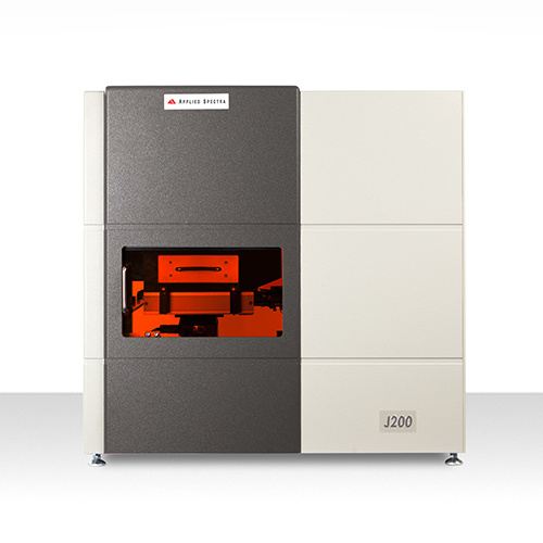
北京富尔邦科技发展有限责任公司为您提供《CuIn1-xGaxSe2太阳能电池薄膜中In、Ga、Mo检测方案(激光诱导击穿)》,该方案主要用于太阳能电池中In、Ga、Mo检测,参考标准--,《CuIn1-xGaxSe2太阳能电池薄膜中In、Ga、Mo检测方案(激光诱导击穿)》用到的仪器有美国ASI 激光诱导击穿光谱仪(LIBS)
相关方案
更多
该厂商其他方案
更多