


方案详情
文
This note demonstrates that depending on the configuration of the Raman system used, one can extract different types of information about Carbon Nanotubes. A multiexcitation, low frequency, high spectral and spatial resolution Raman system is the best solution to collect the maximum information. Raman has shown a high potential in characterising the SWCNTs ‘ structure. The correlation between knowledge about structure with physical and chemical properties about the tubes make the technique extremely powerful to control the quality of the SWCNTs for specific applications. Raman spectrometer capabilities like spatial resolution, spectral resolution and excitation wavelength versatility have been examined. Beside Raman, preliminary fluorescence studies are describing the potential of the technique.
方案详情

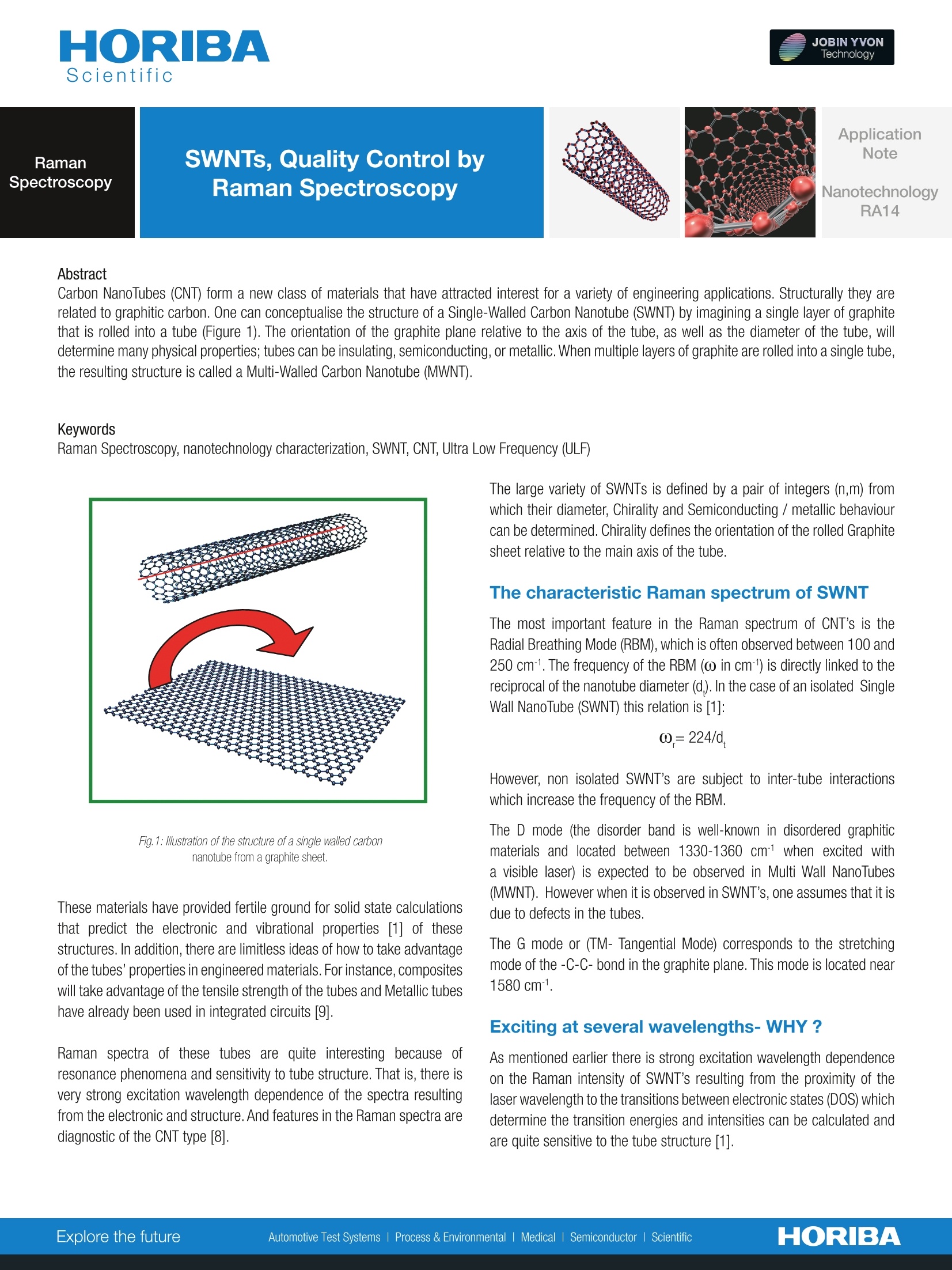
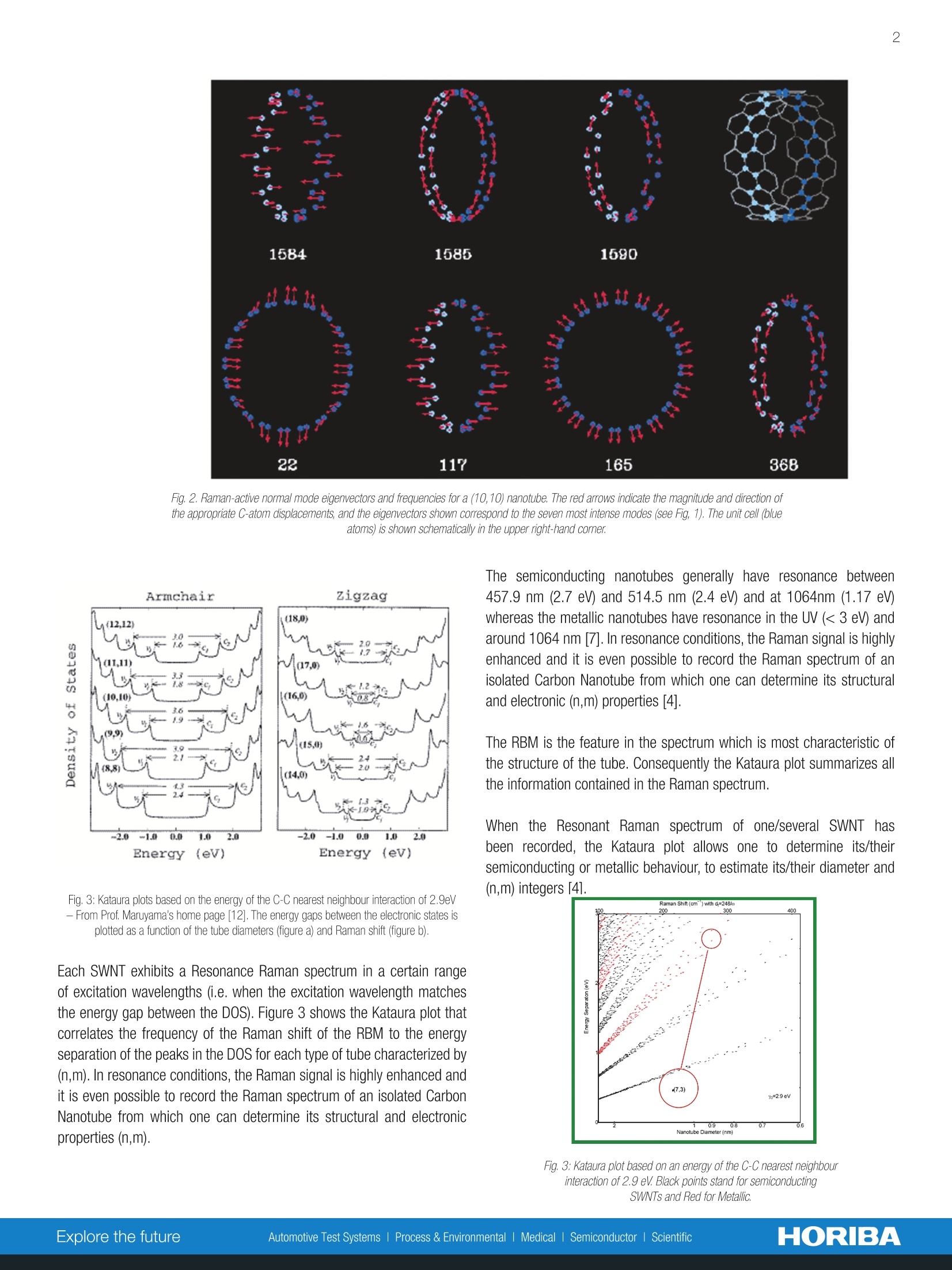
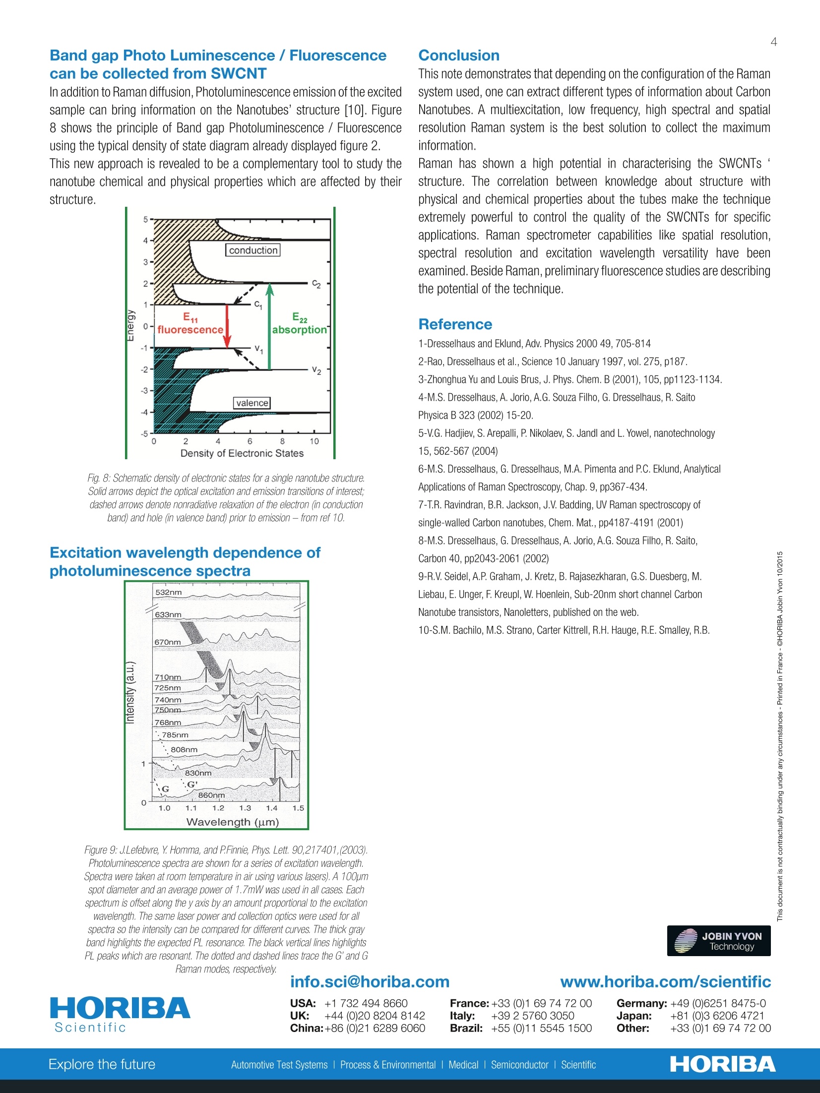
HORIBAScientific 3 RamanSpectroscopy SWNTs, Quality Control byRaman Spectroscopy ApplicationNoteNanotechnologyRA14 Abstract Carbon NanoTubes (CNT) form a new class of materials that have attracted interest for a variety of engineering applications. Structurally they arerelated to graphitic carbon. One can conceptualise the structure of aSingle-Walled Carbon Nanotube (SWNT) by imagining a single layer of graphitethat is rolled into a tube (Figure 1). The orientation of the graphite plane relative to the axis of the tube, as well as the diameter of the tube, willdetermine many physical properties; tubes can be insulating, semiconducting, or metallic. When multiple layers of graphite are rolled into a single tube,the resulting structure is called a Multi-Walled Carbon Nanotube (MWNT). Keywords Fig.1: ustration of the structure of a single walled carbonnanotube from a graphite sheet. These materials have provided fertile ground for solid state calculationsthat predict the electronic and vibrational properties [1] of thesestructures. In addition, there are limitless ideas of how to take advantageof the tubes’ properties in engineered materials. For instance, compositeswill take advantage of the tensile strength of the tubes and Metallic tubeshave already been used in integrated circuits [9]. Raman spectra of these tubes are quite interesting because ofresonance phenomena and sensitivity to tube structure. That is, there isvery strong excitation wavelength dependence of the spectra resultingfrom the electronic and structure. And features in the Raman spectra arediagnostic of the CNT type [8]. The large variety of SWNTs is defined by a pair of integers (n,m) fromwhich their diameter, Chirality and Semiconducting/ metallic behaviourcan be determined. Chirality defines the orientation of the rolled Graphitesheet relative to the main axis of the tube. The characteristic Raman spectrum of SWNT The most important feature in the Raman spectrum of CNT’s is theRadial Breathing Mode (RBM), which is often observed between 100 and250 cm1. The frequency of the RBM ( in cm-1) is directly linked to thereciprocal of the nanotube diameter (d). In the case of an isolated SingleWall NanoTube (SWNT) this relation is [1]: However, non isolated SWNT’s are subject to inter-tube interactionswhich increase the frequency of the RBM. The D mode (the disorder band is well-known in disordered graphiticmaterials and located between 1330-1360 cm1 when excited witha visible laser) is expected to be observed in Multi Wall NanoTubes(MWNT). However when it is observed in SWNT’s, one assumes that it isdue to defects in the tubes. The G mode or (TM-Tangential Mode) corresponds to the stretchingmode of the -C-C-bond in the graphite plane. This mode is located near1580 cm1. Exciting at several wavelengths- WHY ? As mentioned earlier there is strong excitation wavelength dependenceon the Raman intensity of SWNT's resulting from the proximity of thelaser wavelength to the transitions between electronic states (DOS) whichdetermine the transition energies and intensities can be calculated andare quite sensitive to the tube structure [1]. Fig. 2. Raman-active normal mode eigenvectors and frequencies for a (10,10) nanotube. The red arrows indicate the magnitude and direction ofthe appropriate C-atom displacements, and the eigenvectors shown correspond to the seven most intense modes (see Fig,1). The unit cell (blueatoms) is shown schematically in the upper right-hand corner. Fig. 3: Kataura plots based on the energy of the C-C nearest neighbour interaction of 2.9eV-From Prof. Maruyama's home page [12]. The energy gaps between the electronic states isplotted as a function of the tube diameters (figure a) and Raman shift (figure b). Each SWNT exhibits a Resonance Raman spectrum in a certain rangeof excitation wavelengths (i.e. when the excitation wavelength matchesthe energy gap between the DOS). Figure 3 shows the Kataura plot thatcorrelates the frequency of the Raman shift of the RBM to the energyseparation of the peaks in the DOS for each type of tube characterized by(n,m). In resonance conditions, the Raman signal is highly enhanced andit is even possible to record the Raman spectrum of an isolated CarbonNanotube from which one can determine its structural and electronicproperties (n,m). The semiconducting nanotubes generally have resonance between457.9 nm (2.7 eV) and 514.5 nm(2.4 eV) and at 1064nm (1.17 eV)whereas the metallic nanotubes have resonance in the UV (<3 eV) andaround 1064 nm [7]. In resonance conditions, the Raman signal is highlyenhanced and it is even possible to record the Raman spectrum of anisolated Carbon Nanotube from which one can determine its structuraland electronic (n,m) properties [4]. The RBM is the feature in the spectrum which is most characteristic ofthe structure of the tube. Consequently the Kataura plot summarizes allthe information contained in the Raman spectrum. When the Resonant Raman spectrum of one/several SWNT hasbeen recorded, the Kataura plot allows one to determine its/theirsemiconducting or metallic behaviour, to estimate its/their diameter and(n,m) integers [41. Fig. 3: Kataura plot based on an energy of the C-C nearest neighbourinteraction of 2.9 eV. Black points stand for semiconductingSWNTs and Red for Metallic. There is currently no way to synthesize selectively one kind of SWNT witha fixed diameter d and orientation (n,m). Exciting at several wavelengthsallows to sweep several resonance conditions in order to point outselectively the existence of various carbon nanotubes in the sample. Figure 4 clearly demonstrates that this procedure is a good way toenhance selectively the Raman spectrum of different SWNTs [6]. Fig.4: Spectra recorded on the surface of a powder of SWNTs Need of spectral resolution- WHY ? High Spectral Resolution is needed to separate very close modes inthe spectrum of a single nanotube or in the spectrum of a bundle ofnanotubes. Figure 5 shows a RBM spectrum that represents tubes withat least 3 different properties: Fig. 5: Sample bundle of SWNTs 600 gr/mm and 1800 gr/mm on aLabram at 633 nm with power of 0.08 mW.NB: even better spectralresolution can be reached on a Labram HR Need of spatial resolution- WHY ? Using resonant conditions in Raman micro-spectroscopy, the spectrumof a single isolated SWNT can be detected. The difficulty for thoseexperiments is to localise the nanotube on the surface. Probing a largearea of the substrate by the mean of a map is often the only way to findthe"hot spot"[2,5]. Fig 6: In the map ofFigure 6, three RBM frequencies positions are plotted to see the distributionof the different tube diameters. The tubes in this work are scattered on a silicon substrate andare around 0.8 nm to 1.5 nm in diameter.Despite the fact that the laser spot is much larger than the tube diameter the resonance behaviour of the tubes allows the spectra to be recorded. The effect of increasing temperature The light absorption coefficient of the sample depends on the wavelengthof the excitation source. If the light absorption coefficient is high, this maylead to an increase of the temperature in the material and sometimes todamage of the sample. Therefore, it is necessary to reduce the powerdensity at the sample. It is very easy to monitor whether a frequency shiftoccurs. The temperature changes in carbon nanotube induce frequencydown shifts. The amplitude of the shift varies for each mode. For example,the G band follows a downshift of 0.026 cm1.K-1in a MultiWall NanoTube. An experiment has been performed by measuring a spectrum first at lowpower density and then at high power density. Dramatic spectral changesoccur when the laser power increases and those modifications can bepartially reversible. The effect is mainly due to a decrease in the quantityof defects, as shown in figure 7; the D band clearly disappears after theheat treatment. For samples that are particularly sensitive to laser powera line-scan feature can be employed. This feature can also be employedto decrease the time required to map a sample. Figure7 : All the spectra are recorded on the same point on a powderof SWNTs. Source 532 nm. Objective 100x (NA=0.9). Blue: spectrumrecorded with a 0.007mW. Orange: spectrum recorded with a powerof 7mW. Green: spectrum recorded at 0.007 mW after a 30mn cooling.Red: spectrum recorded at 7mW. Band gap Photo Luminescence / Fluorescencecan be collected from SWCNT In addition to Raman diffusion, Photoluminescence emission of the excitedsample can bring information on the Nanotubes’ structure [10]. Figure8 shows the principle of Band gap Photoluminescence / Fluorescenceusing the typical density of state diagram already displayed figure 2. This new approach is revealed to be a complementary tool to study thenanotube chemical and physical properties which are affected by theirstructure. Fig. 8: Schematic density of electronic states for a single nanotube structure.Solid arrows depict the optical excitation and emission transitions of interest;dashed arrows denote nonradiative relaxation of the electron (in conductionband) and hole (in valence band) prior to emission - from ref 10. Excitation wavelength dependence ofphotoluminescence spectra Figure 9: J.Lefebvre, Y. Homma, and P.Finnie, Phys. Lett. 90,217401,(2003).Photoluminescence spectra are shown for a series of excitation wavelength.Spectra were taken at room temperature in air using various lasers). A 100umspot diameter and an average power of 1.7mW was used in all cases. Eachspectrum is offset along the y axis by an amount proportional to the excitationwavelength. The same laser power and collection optics were used for allspectra so the intensity can be compared for different curves. The thick grayband highlights the expected PL resonance. The black vertical lines highlightsPL peaks which are resonant. The dotted and dashed lines trace the G'and G Raman modes, respectively. Conclusion This note demonstrates that depending on the configuration of the Ramansystem used, one can extract different types of information about CarbonNanotubes. A multiexcitation, low frequency, high spectral and spatialresolution Raman system is the best solution to collect the maximuminformation. Raman has shown a high potential in characterising the SWCNTs ‘structure. The correlation between knowledge about structure withphysical and chemical properties about the tubes make the techniqueextremely powerful to control the quality of the SWCNTs for specificapplications. Raman spectrometer capabilities like spatial resolution,spectral resolution and excitation wavelength versatility have beenexamined. Beside Raman, preliminary fluorescence studies are describingthe potential of the technique. Reference 1-Dresselhaus and Eklund, Adv. Physics 2000 49,705-814 ( 2-Rao,Dresselhaus et al . , Science 10 January 1997, vol. 275, p187. ) ( 3-Zhonghua Yu and Louis Brus, J . Phys. C hem. B (2001), 1 0 5, pp1123-1134. ) 4-M.S. Dresselhaus, A. Jorio, A.G. Souza Filho, G.Dresselhaus, R. SaitoPhysica B 323 (2002) 15-20. 5-V.G. Hadjiev, S. Arepalli, P. Nikolaev, S. Jandl and L. Yowel, nanotechnology15,562-567 (2004) 6-M.S. Dresselhaus, G. Dresselhaus, M.A. Pimenta and P.C. Eklund, AnalyticalApplications of Raman Spectroscopy, Chap.9, pp367-434. ( 7 -T.R. Ravindran, B.R. Jackson,J.V. Badding, UV Raman spectroscopy of s ingle-walled Carbon n anotubes, Chem. Mat., pp4187-419 1 (2001) ) ( 8-M.S. Dresselhaus, G. Dresselhaus, A. Jorio,A.G. Souza Filho, R. S aito, Carbon 40, pp2043-2061 (2002) ) ( 9-R.V. Seidel, A.P. Graham,J. K retz, B. Rajasez k haran, G.S. Duesberg, M .L iebau,E . Unger, F . K reupl, W. H oenlein, S ub-20nm short channel Car b onNanotube transistors, Nanoletters, published on the web. ) ( 1 0-S.M. Bachilo, M . S. Strano, Ca r ter Kittrell, R .H. H aug e , R . E. Smalley, R.B. ) USA: +1 732 494 8660 UK: +44 (0)20 82048142 France:+33 (0)169 74 72 00Germany: +49 (0)6251 8475-0Italy: +39 25760 3050Japan: +81 (0)3 6206 4721Brazil: +55(0)11 5545 1500Other: +33(0)1 69 74 72 00 HORIBAExplore the futureAutomotive Test Systems IProcess & EnvironmentalillMedicalSemiconductor Scientific This note demonstrates that depending on the configuration of the Raman system used, one can extract different types of information about Carbon Nanotubes. A multiexcitation, low frequency, high spectral and spatial resolution Raman system is the best solution to collect the maximum information. Raman has shown a high potential in characterising the SWCNTs ‘ structure. The correlation between knowledge about structure with physical and chemical properties about the tubes make the technique extremely powerful to control the quality of the SWCNTs for specific applications. Raman spectrometer capabilities like spatial resolution, spectral resolution and excitation wavelength versatility have been examined. Beside Raman, preliminary fluorescence studies are describing the potential of the technique.
确定

还剩2页未读,是否继续阅读?

HORIBA(中国)为您提供《碳纳米管中结构(手性等),化学性质检测方案(激光拉曼光谱)》,该方案主要用于纳米材料中结构(手性等),化学性质检测,参考标准--,《碳纳米管中结构(手性等),化学性质检测方案(激光拉曼光谱)》用到的仪器有
相关方案
更多
该厂商其他方案
更多