


方案详情
文
HORIBAScientific研发的拉曼光谱仪可与多个知名厂家的AFM/STM / NSOM联用,根据您的选择为您提供一个多功能、可靠的解决方案。 ⊕进行AFM微区形貌扫描的同时,同步进行拉曼扫描成像 ⊕针尖增强拉曼光谱(TERS)测试 ⊕多种耦连方式:底部/顶部/侧向照射
方案详情

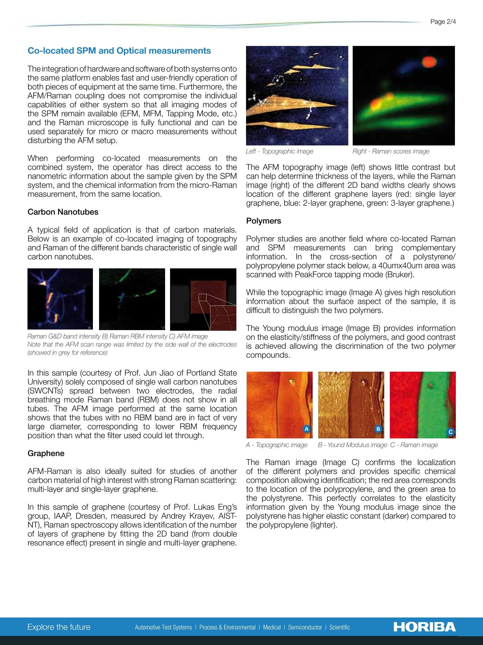
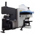
HORIBAScientific Page 2/4 AFM-Raman Coupling and Tip-Enhanced Raman (TERS) Raman microscopy has become an essential tool for the analysis of materials on the micron and even sub-micronscale. HORIBA Scientific's expertise in optical and mechanical design insures that HORIBA Raman instrumentsreach the optimal spatial resolution. The advent of Scanning Probe Microscopy techniques (SPM)such as Atomic Force Microscopy (AFM) and ScanningTunneling Microscopy (STM), which allow measurement oftopography, adhesion, electro-magnetic or electro-chemicalproperties and many other types of analysis at the nanometricscale, have benefitted innumerable fields of scientific research,especially material scientists and molecular biologists. Coupling the two techniques (SPM and spectroscopy) soonbecame attractive in order to identify chemical compositionof nano-objects of interest, or simply to establish the object'slocation through spectroscopic means before proceedingto characterization with near-field methods. Those co-localized measurements are particularly powerful with nano-objects showing strong Raman scattering such as carbonnanotubes, nanowires, and graphene or those showingstrong luminescence like quantum dots. The need for chemical characterization techniques to reachhigher spatial resolution also became clear, however if near-field scanning optical microscopy (NSOM) brought relativesuccess in detecting strong signals like in absorptionspectroscopy or photoluminescence, obtaining specificchemicalinformation) at the nano-scale withRamanspectroscopy only became realistic with the development oftip-enhanced Raman scattering (TERS). TERS takes advantage of surface plasmon resonance,dipole and chemical resonance effects, using special metalcoatings on the SPM probe tip greatly enhancing the Ramanscattering from the near-field directly under the probe. Thisenhanced near-field signal is then collected along with the far-field signal that can be discriminated against using differenttechniques, so as to extract the near-field Raman signal andgenerate nano-scale Raman profile or images. The optical coupling to the SPM/AFM system essentiallydepends on the configuration of the SPM and its purpose.SPM systems designed for the biological field usually fit ona standard inverted optical microscope, while coupling to Figure 1: Different illumination/collection schemes SPM systems designed for opaque samples depends on theSPM optical access. Top illumination is often possible and ispreferred for co-localized measurements, but the shadowingeffect from the cantilever limits TERS to the use of transparentprobes or extended tips, so that oblique (side) illumination isrequired for use of standard metal-coated tips. HORIBA the leader in Spectroscopy teams up withthe leaders in SPM HORIBA Scientific partners with the leading SPM companiesin the world to provide the best combined instrument for theapplication. Different partners offer different capabilities andlend their mastery in various fields of applications. HORIBAmarries its expertise in Spectroscopy together with that ofthe major suppliers in the field of Scanning Probe Microscopyproducing the highest performing instruments on the market. HORIBA Scientific offers AFM coupling options for top,bottom and oblique illumination schemes (figure 1) to usewith its high-spectral-resolution Raman microscope LabramHR as well as the more compact XploRA, in both their uprightand inverted microscope versions, allowing coupling to awide range of SPM systems (see compatibility chart below). The integration of hardware and software of both systems ontothe same platform enables fast and user-friendly operation ofboth pieces of equipment at the same time. Furthermore, theAFM/Raman coupling does not compromise the individualcapabilities of either system so that all imaging modes ofthe SPM remain available (EFM, MFM, Tapping Mode, etc.)and the Raman microscope is fully functional and can beused separately for micro or macro measurements withoutdisturbing the AFM setup. When performingco-locatedmeasurements on thecombined system, the operator has direct access to thenanometric information about the sample given by the SPMsystem, and the chemical information from the micro-Ramanmeasurement, from the same location. Carbon Nanotubes A typical field of application is that of carbon materials.Below is an example of co-located imaging of topographyand Raman of the different bands characteristic of single wallcarbon nanotubes. Raman G&D band intensity B) Raman RBM intensity C) AFM imageNote that the AFM scan range was limited by the side wall of the electrodes(showed in grey for reference) In this sample (courtesy of Prof. Jun Jiao of Portland StateUniversity) solely composed of single wall carbon nanotubes(SWCNTs) spread between two electrodes, the radialbreathing mode Raman band (RBM) does not show in alltubes. The AFM image performed at the same locationshows that the tubes with no RBM band are in fact of verylarge diameter, corresponding to lower RBM frequencyposition than what the filter used could let through. Graphene AFM-Raman is also ideally suited for studies of anothercarbon material of high interest with strong Raman scattering:multi-layer and single-layer graphene. In this sample of graphene (courtesy of Prof. Lukas Eng'sgroup, IAAP, Dresden, measured by Andrey Krayev, AlST-NT), Raman spectroscopy allows identification of the numberof layers of graphene by fitting the 2D band (from doubleresonance effect) present in single and multi-layer graphene. Left-Topographic image Right - Raman scores image The AFM topography image (left) shows little contrast butcan help determine thickness of the layers, while the Ramanimage (right) of the different 2D band widths clearly showslocation of the different graphene layers (red: single layergraphene, blue: 2-layer graphene, green: 3-layer graphene.) Polymers Polymer studies are another field where co-located RamanandSPMmeasurementscanbringcomplementaryinformation. In the cross-section ofa polystyrene/polypropylene polymer stack below, a 40umx40um area wasscanned with PeakForce tapping mode (Bruker). While the topographic image (Image A) gives high resolutioninformation about the surface aspect of the sample, it isdifficult to distinguish the two polymers. The Young modulus image (lmage B) provides informationon the elasticity/stiffness of the polymers, and good contrastis achieved allowing the discrimination of the two polymercompounds. A -Topographic image B- Yound Modulus image C-Raman image The Raman image (lmage C) confirms the localizationof the different polymers and provides specific chemicalcomposition allowing identification; the red area correspondsto the location of the polypropylene, and the green area tothe polystyrene. This perfectly correlates to the elasticityinformation given by the Young modulus image since thepolystyrene has higher elastic constant (darker) compared tothe polypropylene (lighter). Tip Enhanced Raman Scattering (TERS) Carbon Nanotubes Surface Enhance Raman Scattering (SERS) has long beenused to enhance weak Raman signals by taking advantageof surface plasmon resonance, and chemical resonance,using nano-particle colloids or rough metallic substrates,allowing detection of chemical species at ppm levels. Carbon nanotubes are ideal samples to illustrate spatialresolution of the TERS technique. In the example below,(courtesy of Mark Chaigneau, Ecole Polytechnique, Razvigorgroup) the STM image shows two aligned multi-wall carbonnanotubes side-by-side. The STM profile across those tubesshows that they are separated by about 70nm. The Ramanprofile of the G band at 1590cm-1 is fitted to determine theapparent width of the tubes, and finds the smaller tube to beabout 30nm diameter. The TERS effect is based on a similar principle, but uses ametal-coated AFM tip(or a single nanoparticle attached tothe tip) as a dipole antenna that enhances the Raman signalcoming from the sample area at the end of the tip (near-field). Although not yet fully understood, the TERS effect hasattracted a lot of interest, as it holds the promise of producingchemical images with nanometric resolution. The different coupling schemes available (figure 1) to performTERS on the Labram HR series or XploRA series offer anideal integrated platform for diverse applications. Softwaredeveloped for communication with SPMs from differentmanufacturers allows seamless integration of the twotechniques while keeping the full capabilities of the individualinstruments. Specific methods were also developed tooptimize laser-tip alignment and maximize throughput. S7M image With these combined expertise, TERS can be approachedwith confidence. Azobenzene STM profile Azobenzene is a good candidate for TERS as it is easilyadsorbed as a monolayer on a gold substrate and barelyexhibits any Raman signal from the far-field, so that whensignal is observed, it is proof that enhancement is occurringand that is proof of TERS. The blue spectrum below shows the far-field Raman signalwith a 30s integration time, while the red spectrum (1sintegration time) is the TERS spectrum. Profile of the Raman G band Silicon Germanium Trench Silicon Germanium (SiGe) is a very popular semiconductorused for microchips, which now have critical dimensionsbelow 50nm. This sample (courtesy of Ecole Polytechnique),contains a 150nm wide by 50nm deep trench of Ge in dopedsilicon. The Raman profile shows the trench is well resolvedwith TERS. TERS spectra tip up (blue) and tip down (red) STM image Raman profile of Ge bands AFM Compatibility chart SPM Model cooo co co Eb ooEoo coEooo Notes Aist-NT CombiScope √ √ SmartSPM Asylum Research MFP-3D LabRam HR INV or XploRa INV Bruker (Veeco) Catalyst BioScope IRIS LabRam HR INV or XploRa INV Dimension 3100 米 LabRam HR only Innova IRIS JPK NanoWizard ...... 03..0 +....... LabRam HR INV or XploRa INV F........................................ Shuttle Nanonics MV-1000 √* √* √* * TERS using top illumination exclusively with Nanonicstransparent probes * Top and Bottom requires Nanonics Integration package MV-2000 Park Systems MV-4000 XE-70, XE-100, XE-150.....5 ..3.XE-120XE-Bio XE-NSOM 米米米 ....... .... * * .............EO.- * Top and Bottom under different microscopes * Top and Bottom under different microscopes * Park transmission NSOM only Tip-Enhanced (TERS) ready. Also allows co-located SPM and optical measurements Co-localized SPM and optical measurements (Raman, Photoluminescence, Fluorescence, ...) Co-localized SPM and optical measurements; the sample is moved reproducibly between the two techniques SPM systems designed for inverted microscopes are compatible with the Labram HR INV and XploRA INV without anyadditional optics. SPM systems that include their own sampling optics can be coupled to the Labram HR, Labram HR INV and XploRA usingthe microscope horizontal exit port (option). SPM systems that do not include sampling optics can be coupled to the Labram HR, Labram HR INV and XploRA usingthe side coupling optical module (option, which includes horizontal exit port option). info.sci@horiba.comwww.horiba.com/scientific USA:+1732 494 8660 France:+33 (0)1 64 54 1300 Germany: +49(0)89 4623 17-0UK: +44 (0)20 8204 8142 Italy: +39257603050 Japan: +81 (0)3 62064717China:+86 (0)10 8567 9966 Brazil:+55 (0)11 5545 1514Other Countries: +33 (0)1 64 54 1300 JOBIN YVONTechnologyHORIBAExplore the futureAutomotive Test Systems Process & Environmental Medicall SemiconductorIl Scientific
确定
还剩2页未读,是否继续阅读?

产品配置单
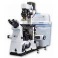
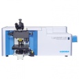
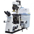
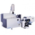
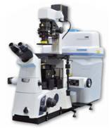
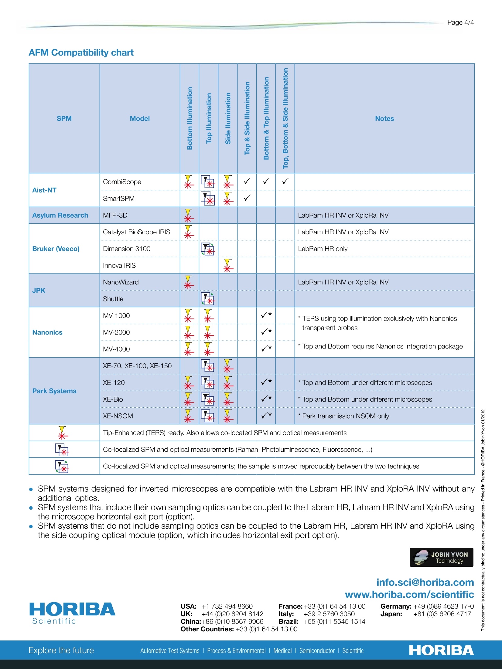
上海巨纳科技有限公司为您提供《AFM-Raman Coupling and Tip-Enhanced Raman (TERS)中AFM-Raman Coupling and Tip-Enhanced Raman (TERS)检测方案 》,该方案主要用于其他中AFM-Raman Coupling and Tip-Enhanced Raman (TERS)检测,参考标准--,《AFM-Raman Coupling and Tip-Enhanced Raman (TERS)中AFM-Raman Coupling and Tip-Enhanced Raman (TERS)检测方案 》用到的仪器有HORIBAXploRA INV智能型全自动拉曼光谱仪、HORIBA HR Evolution高分辨拉曼光谱仪、HORIBACombiscopeXploRA原子力拉曼联用系统、Horiba XploRA INV 多功能拉曼及成像光谱仪、HORIBA T64000三级拉曼光谱仪
相关方案
更多