


方案详情
文
Electron imaging and Raman spectroscopy are established techniques for viewing and analysing carbon nanotubes. Performing these two techniques usually requires the sample being transferred between a scanning electron microscope(SEM) and a Raman spectrometer. This application note illustrates the advantages of Renishaw^^s structural and chemical analyser(SCA) for imultaneous secondary electron imaging and Raman spectroscopy of single-wall carbon anotubes(SWNTs).
方案详情

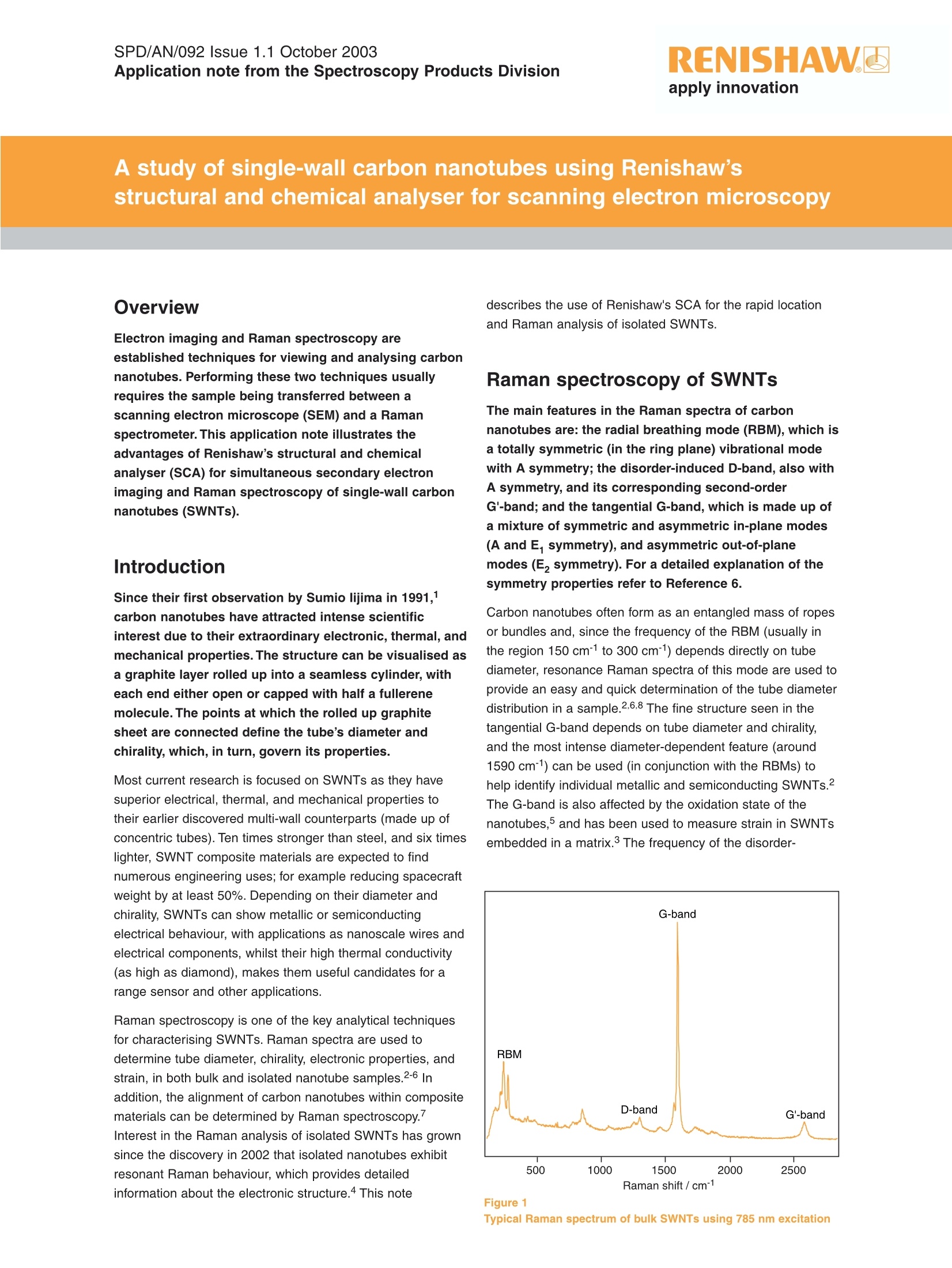
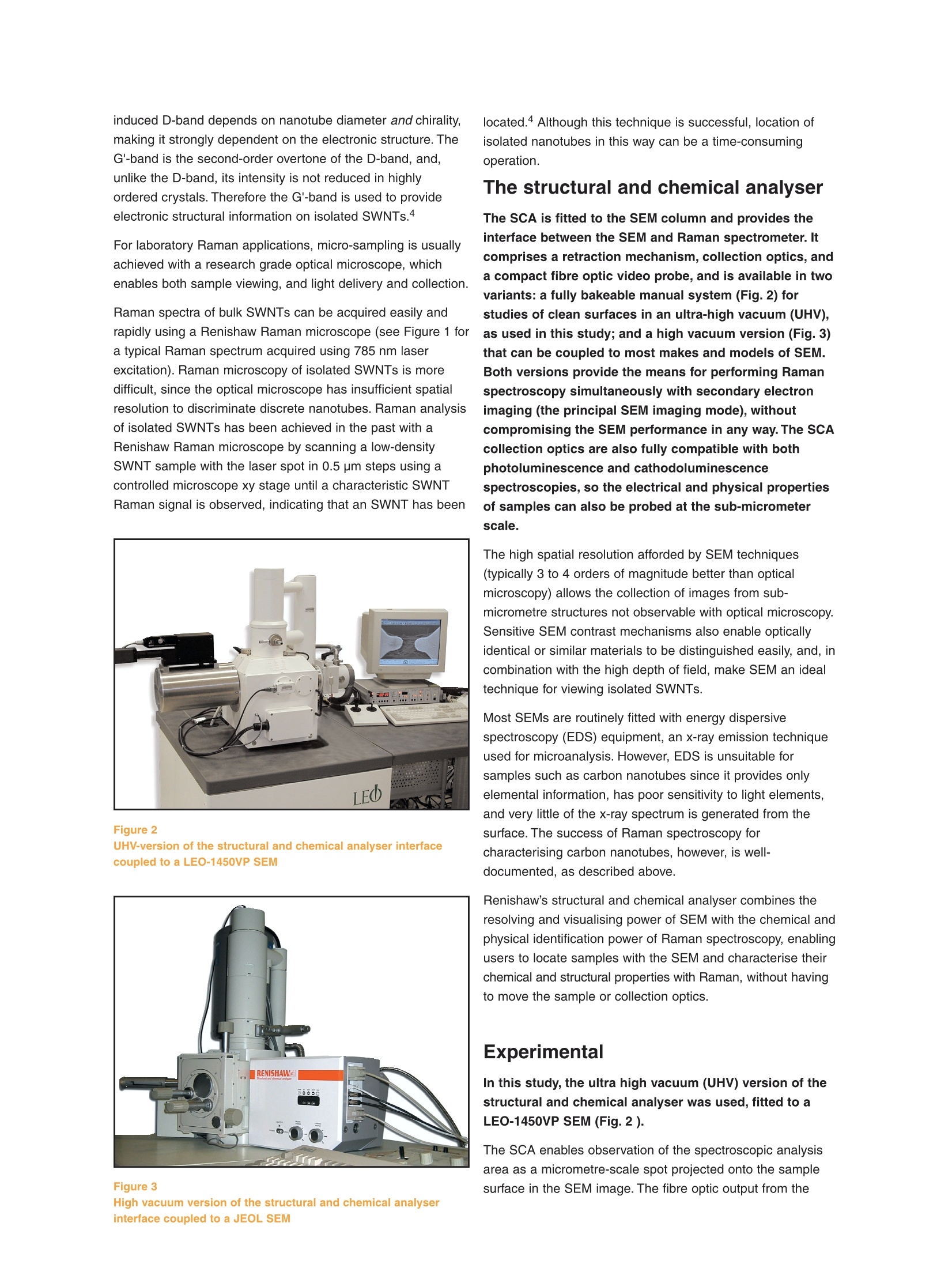
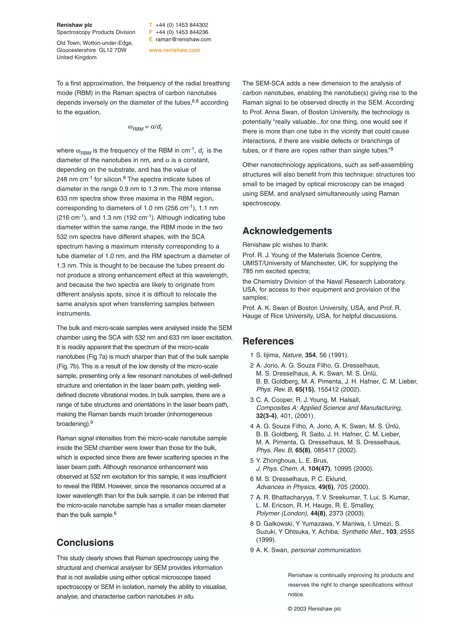
SPD/AN/092 Issue 1.1 October 2003Application note from the Spectroscopy Products Division +44 (0) 1453 844302F +44 (0) 1453 844236E raman@renishaw.comRenishaw plcSpectroscopy Products DivisionOld Town, Wotton-under-Edge,Gloucestershire GL127DWUnited Kingdomwww.renishaw.com A study of single-wall carbon nanotubes using Renishaw’sstructural and chemical analyser for scanning electron microscopy Electron imaging and Raman spectroscopy areestablished techniques for viewing and analysing carbonnanotubes. Performing these two techniques usuallyrequires the sample being transferred between ascanning electron microscope (SEM) and a Ramanspectrometer. This application note illustrates theadvantages of Renishaw's structural and chemicalanalyser (SCA) for simultaneous secondary electronimaging and Raman spectroscopy of single-wall carbonnanotubes (SWNTs). Introduction Since their first observation by Sumio lijima in 1991,carbon nanotubes have attracted intense scientificinterest due to their extraordinary electronic, thermal, andmechanical properties. The structure can be visualised asa graphite layer rolled up into a seamless cylinder, witheach end either open or capped with half a fullerenemolecule. The points at which the rolled up graphitesheet are connected define the tube's diameter andchirality, which, in turn, govern its properties. Most current research is focused on SWNTs as they havesuperior electrical, thermal, and mechanical properties totheir earlier discovered multi-wall counterparts (made up ofconcentric tubes). Ten times stronger than steel,and six timeslighter, SWNT composite materials are expected to findnumerous engineering uses; for example reducing spacecraftweight by at least 50%. Depending on their diameter andchirality, SWNTs can show metallic or semiconductingelectrical behaviour, with applications as nanoscale wires andelectrical components, whilst their high thermal conductivity(as high as diamond), makes them useful candidates for arange sensor and other applications. Raman spectroscopy is one of the key analytical techniquesfor characterising SWNTs. Raman spectra are used todetermine tube diameter, chirality, electronic properties, andstrain, in both bulk and isolated nanotube samples.2-6 Inaddition, the alignment of carbon nanotubes within compositematerials can be determined by Raman spectroscopy.Interest in the Raman analysis of isolated SWNTs has grownsince the discovery in 2002 that isolated nanotubes exhibitresonant Raman behaviour, which provides detailedinformation about the electronic structure.4 This note describes the use of Renishaw's SCA for the rapid locationand Raman analysis of isolated SWNTs. Raman spectroscopy of SWNTs The main features in the Raman spectra of carbonnanotubes are: the radial breathing mode (RBM), which isa totally symmetric (in the ring plane) vibrational modewith A symmetry; the disorder-induced D-band, also withA symmetry, and its corresponding second-orderG'-band; and the tangential G-band, which is made up ofa mixture of symmetric and asymmetric in-plane modes(A and E symmetry), and asymmetric out-of-planemodes (E, symmetry). For a detailed explanation of thesymmetry properties refer to Reference 6. Carbon nanotubes often form as an entangled mass of ropesor bundles and, since the frequency of the RBM (usually inthe region 150 cm-1 to 300 cm-1) depends directly on tubediameter, resonance Raman spectra of this mode are used toprovide an easy and quick determination of the tube diameterdistribution in a sample.2,6,8The fine structure seen in thetangential G-band depends on tube diameter and chirality,and the most intense diameter-dependent feature (around1590 cm-1) can be used (in conjunction with the RBMs) tohelp identify individual metallic and semiconducting SWNTs.The G-band is also affected by the oxidation state of thenanotubes,5 and has been used to measure strain in SWNTsembedded in a matrix.3 The frequency of the disorder- Raman shift /cm1 Figure 1 induced D-band depends on nanotube diameter and chirality,making it strongly dependent on the electronic structure. TheG'-band is the second-order overtone of the D-band, and,unlike the D-band, its intensity is not reduced in highlyordered crystals. Therefore the G'-band is used to provideelectronic structural information on isolated SWNTs.4 For laboratory Raman applications, micro-sampling is usuallyachieved with a research grade optical microscope, whichenables both sample viewing, and light delivery and collection. Raman spectra of bulk SWNTs can be acquired easily andrapidly using a Renishaw Raman microscope (see Figure 1 fora typical Raman spectrum acquired using 785 nm laserexcitation). Raman microscopy of isolated SWNTs is moredifficult, since the optical microscope has insufficient spatialresolution to discriminate discrete nanotubes. Raman analysisof isolated SWNTs has been achieved in the past with aRenishaw Raman microscope by scanning a low-densitySWNT sample with the laser spot in 0.5 pm steps using acontrolled microscope xy stage until a characteristic SWNTRaman signal is observed, indicating that an SWNT has been Figure 2 UHV-version of the structural and chemical analyser interfacecoupled to a LEO-1450VP SEM located.4 Although this technique is successful, location ofisolated nanotubes in this way can be atime-consumingoperation. The structural and chemical analyser The SCA is fitted to the SEM column and provides theinterface between the SEM and Raman spectrometer. Itcomprises a retraction mechanism, collection optics, anda compact fibre optic video probe, and is available in twovariants: a fully bakeable manual system (Fig.2) forstudies of clean surfaces in an ultra-high vacuum (UHV)as used in this study; and a high vacuum version (Fig.3)that can be coupled to most makes and models of SEM.Both versions provide the means for performing Ramanspectroscopy simultaneously with secondary electronimaging (the principal SEM imaging mode), withoutcompromising the SEM performance in any way. The SCAcollection optics are also fully compatible with bothphotoluminescence and cathodoluminescencespectroscopies, so the electrical and physical propertiesof samples can also be probed at the sub-micrometerscale. The high spatial resolution afforded by SEM techniques(typically 3 to 4 orders of magnitude better than opticalmicroscopy) allows the collection of images from sub-micrometre structures not observable with optical microscopy.Sensitive SEM contrast mechanisms also enable opticallyidentical or similar materials to be distinguished easily, and, incombination with the high depth of field, make SEM an idealtechnique for viewing isolated SWNTs. Most SEMs are routinely fitted with energy dispersivespectroscopy (EDS)equipment, an x-ray emission techniqueused for microanalysis. However, EDS is unsuitable forsamples such as carbon nanotubes since it provides onlyelemental information, has poor sensitivity to light elements,and very little of the x-ray spectrum is generated from thesurface. The success of Raman spectroscopy forcharacterising carbon nanotubes, however, is well-documented, as described above. Renishaw's structural and chemical analyser combines theresolving and visualising power of SEM with the chemical andphysical identification power of Raman spectroscopy,enablingusers to locate samples with the SEM and characterise theirchemical and structural properties with Raman, without havingto move the sample or collection optics. Experimental In this study, the ultra high vacuum (UHV) version of thestructural and chemical analyser was used, fitted to aLEO-1450VP SEM (Fig.2). The SCA enables observation of the spectroscopic analysisarea as a micrometre-scale spot projected onto the samplesurface in the SEM image. The fibre optic output from the SCA was connected to a Renishaw RM1000 spectrometerunit for spectral analysis, equipped with 532 nm and 633 nmlaser excitation. Two samples were analysed: a bulk sample consisting of anentangled mass of nanotubes having a ‘matted'appearance,and a micro-scale sample comprising discrete nanotubesaligned between two gold electrodes, 1 pm apart (Fig.4). Figure 4SEM image of nanotubes aligned between two electrodes Different excitation wavelengths interact differently with carbonnanotubes, depending on the nanotubes' size and properties,so Raman spectra were acquired from both samples using532 nm and 633 nm laser excitation. As a control, the bulksample was also analysed using a standard Renishaw Ramanmicroscope, employing a research grade optical microscopesystem and the same RM1000 spectrometer unit and lasersas above: the sample was viewed with white light beforeswitching to the laser beam for Raman analysis. The spatialresolution of the optical microscope proved insufficient toimage discrete nanotubes in either the bulk or micro-scalesample. Results and discussion Raman spectra from the bulk sample were acquired frominside the SEM chamber, and from the optical microscopesystem using 532 nm and 633 nm excitation, and confirm thatthe same spectral resolution is achieved with the SCA (Figs5a and 6a) as with the optical microscope system (Figs 5band 6b). The two spectra taken using 633 nm radiation (Fig.6)were 3 to 4 times more intense than the 532 nm excitedspectra (Fig. 5), clearly showing resonance enhancement. Raman shift/cm Figure 5 Raman spectra of bulk carbon nanotubes acquired using 532 nmexcitation with a) the SCA, and b) conventional sampling underthe optical microscope system. Note: the efficiency of Raman scattering varies approximatelywith v4, where v is the frequency of the excitation wavelength.Therefore a two-fold increase in signal intensity would beexpected in changing from 532 nm to 633 nm alone, with theremainder of the increase being caused by resonance effects. Raman shift /cm Raman shift/cm Figure 7 Raman spectra of bulk carbon nanotubes acquired using 633 nmexcitation with a) the SCA, and b) conventional sampling underthe optical microscope system. Raman spectra of a) discrete, and b) bulk, carbon nanotubesamples, acquired using 532 nm excitation. To a first approximation, the frequency of the radial breathingmode (RBM) in the Raman spectra of carbon nanotubesdepends inversely on the diameter of the tubes,6,8 accordingto the equation, where ωRBM is the frequency of the RBM in cm-1, d, is thediameter of the nanotubes in nm, and a is a constant,depending on the substrate, and has the value of248 nm cm-1 for silicon.8 The spectra indicate tubes ofdiameter in the range 0.9 nm to 1.3 nm. The more intense633 nm spectra show three maxima in the RBM region,corresponding to diameters of 1.0 nm (256 cm-1), 1.1 nm(216 cm-1), and 1.3 nm(192 cm-1). Although indicating tubediameter within the same range, the RBM mode in the two532 nm spectra have different shapes, with the SCAspectrum having a maximum intensity corresponding to atube diameter of 1.0 nm, and the RM spectrum a diameter of1.3 nm. This is thought to be because the tubes present donot produce a strong enhancement effect at this wavelength,and because the two spectra are likely to originate fromdifferent analysis spots, since it is difficult to relocate thesame analysis spot when transferring samples betweeninstruments. The bulk and micro-scale samples were analysed inside the SEMchamber using the SCA with 532 nm and 633 nm laser excitation.It is readily apparent that the spectrum of the micro-scalenanotubes (Fig 7a) is much sharper than that of the bulk sample(Fig.7b). This is a result of the low density of the micro-scalesample, presenting only a few resonant nanotubes of well-definedstructure and orientation in the laser beam path, yielding well-defined discrete vibrational modes. In bulk samples, there are arange of tube structures and orientations in the laser beam path,making the Raman bands much broader (inhomogeneousbroadening). Raman signal intensities from the micro-scale nanotube sampleinside the SEM chamber were lower than those for the bulk,which is expected since there are fewer scattering species in thelaser beam path. Although resonance enhancement wasobserved at 532 nm excitation for this sample, it was insufficientto reveal the RBM. However, since the resonance occurred at alower wavelength than for the bulk sample, it can be inferred thatthe micro-scale nanotube sample has a smaller mean diameterthan the bulk sample. Conclusions This study clearly shows that Raman spectroscopy using thestructural and chemical analyser for SEM provides informationthat is not available using either optical microscope basedspectroscopy or SEM in isolation, namely the ability to visualise,analyse, and characterise carbon nanotubes in situ. The SEM-SCA adds a new dimension to the analysis ofcarbon nanotubes, enabling the nanotube(s) giving rise to theRaman signal to be observed directly in the SEM. Accordingto Prof. Anna Swan, of Boston University, the technology ispotentially “really valuable...for one thing, one would see ifthere is more than one tube in the vicinity that could causeinteractions, if there are visible defects or branchings oftubes, or if there are ropes rather than single tubes. Other nanotechnology applications, such as self-assemblingstructures will also benefit from this technique: structures toosmall to be imaged by optical microscopy can be imagedusing SEM, and analysed simultaneously using Ramanspectroscopy. Acknowledgements Renishaw plc wishes to thank: Prof. R. J.Young of the Materials Science Centre,UMIST/University of Manchester, UK, for supplying the785nm excited spectra; the Chemistry Division of the Naval Research Laboratory,USA, for access to their equipment and provision of thesamples; Prof. A. K. Swan of Boston University, USA, and Prof. R.Hauge of Rice University, USA, for helpful discussions. References 1 S. lijima, Nature, 354, 56 (1991). ( 2 A. Jorio, A. G. Souza Filho, G. Dresselhaus, M. S . Dresselhaus, A. K. S wan, M. S . Unlu, B. B. Goldberg, M. A. Pimenta, J . H. Hafner, C. M. Lieber,Phys. Rev. B, 65(15), 155412 ( 2002). ) 3 C. A. Cooper, R. J.Young, M. Halsall,Composites A:Applied Science and Manufacturing,32(3-4),401,(2001). 4 A. G. Souza Filho, A. Jorio, A. K. Swan, M. S.Unlu,B. B. Goldberg, R. Saito, J. H. Hafner, C. M. Lieber,M. A. Pimenta, G. Dresselhaus, M. S.Dresselhaus,Phys. Rev. B, 65(8), 085417 (2002). 5 Y. Zhonghoua, L. E. Brus,J. Phys. Chem.A, 104(47), 10995 (2000). ( 6 M . S . Dresselhaus,P . C. Eklund, Advances in P h ysics, 49(6), 705 ( 2 000). ) 7 A. R. Bhattacharyya, T. V. Sreekumar, T. Lui, S. Kumar,L. M. Ericson, R. H. Hauge, R. E. Smalley,Polymer (London),44(8),2373(2003). 8 D. Galkowski, Y. Yumazawa,Y. Maniwa, I.Umezi, S.Suzuki, Y Ohtsuka, Y. Achiba, Synthetic Met., 103, 2555(1999). 9 A. K. Swan, personal communication. Renishaw is continually improving its products andreserves the right to change specifications withoutnotice. Figure
确定

还剩2页未读,是否继续阅读?

产品配置单

英国雷尼绍公司(Renishaw)展位为您提供《A study of single-wall carbon nanotubes using Renishaw^s structural and chemical analyser for scanning electron microscopy》,该方案主要用于碳材料中--检测,参考标准--,《A study of single-wall carbon nanotubes using Renishaw^s structural and chemical analyser for scanning electron microscopy》用到的仪器有inVia Reflex显微拉曼光谱仪
相关方案
更多