产地类别: 进口
美国Hummingbird是电镜业内最知名的原位透射应用厂家至今已有10年的原位透射研发经验,蜂鸟来源于著名的柏克林国家实验室,其专利的技术如液体样品杆,气氛反应样品杆,加热样品杆得到电镜工作者广泛的认可。


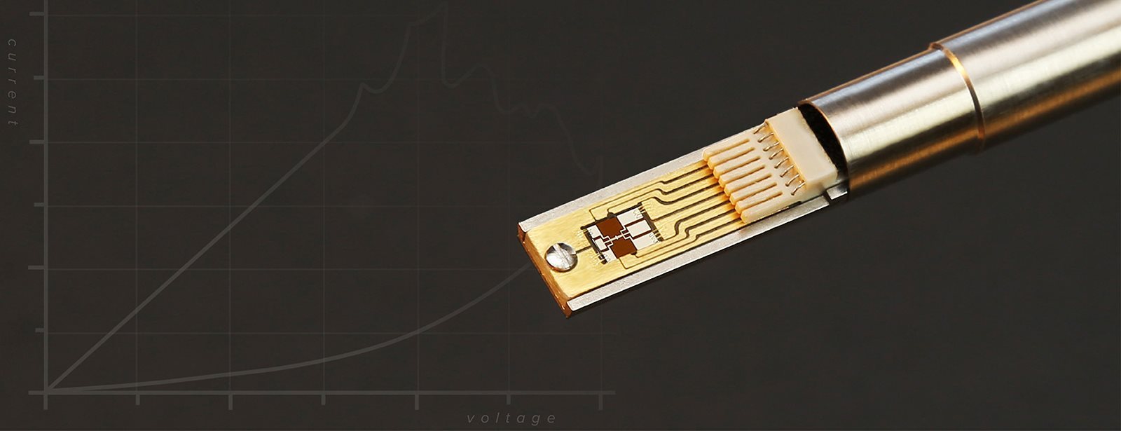
Board Contact (Type I)
This contact configuration has a conveniently removable reusable sample carrier onto which the chip is mounted.
Direct Chip Contact (Type II)
This contact configuration has a unique single chip that is directly inserted in the holder in a proprietary connector with up to 9 electrical contacts.
Spring Contact (Type III)
The spring contact configuration is a variation of the Type I connector that has fixed location spring contacts between the chip and the carrier.
Application Examples
?Correlating electrical properties of nanoscale material with microstructure ?Relating material defect populations to the electrical response Electromigration studies ?Operating microelectomechanical systems (MEMS)-based mechanical testing devices ?In-situ testing of solid-state energy devices
Options
?The 1600 Series Holder can be customized from a range of options. ?Custom designed sample carriers to fit any TEM sample geometry. ?Standard Bundled Shielded Wiring Option ?Low noise, individually shielded cabling option for pA range current measurements. ?Keithley 2400 SMU
Accessories
?Accessories available to maximize the versatility and ease of use of your Electrical Biasing Holder. ?Specialized Sample Substrate Chips ?Vacuum Tip Cover ?Custom Chip Carriers ?Keithley 2400 SMU
Nanoelectronics
Allowing researchers to perform in-situ TEM electrical measurements is a powerful tool for research into next generation of nano-scale electrical devices. Electrical signals can be applied or measured on individual nano-structures and devices, revealing relations between electrical behavior and microstructure.

Top: TEM images taken in-situ during the
voltage scan in panel, at times I, II, III, and IV. Note the correlation of
resistance with void size.
Bottom: Voltage scan on a single nanowires device (inset). The blue square in the inset shows the location of the TEM observation in panel B.
From Void Formation Induced Electrical Switching in Phase-Change Nanowires, Nano Letters 8, 4562, 2008. Image courtesy of Profs. Yi Cui, Stanford University and Andrew Minor, UC Berkeley.
Specification:
Items | 1600 Series |
Tilt Range | ±45° depending on microscope and pole piece |
Number of Electrical Contacts | 6, 8, or 9 * |
Contact Type | Flexible wirebond contacts or fixed spring contact |
Chip Carrier | Mobile Chip Carrier |
Carrier Compatibility | Standard TEM Sample Supports |
Carrier Size | Fits up to 3 x 6 mm samples |
Wiring | Standard or Low-noise shielded |
TEM Compatibility | FEI, JEOL, Hitachi, Zeiss |

云必真空设备原位进样系统/真空转移盒/原位样品台MUST IN2


高分辨成像与光谱分析阴极发光成像系统Gatan Mono CL4

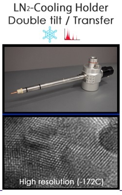
双倾冷冻及真空传输透射电镜样品杆LN2

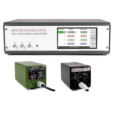
Spicer Consulting 主动式消磁器 SC24/Room Cable

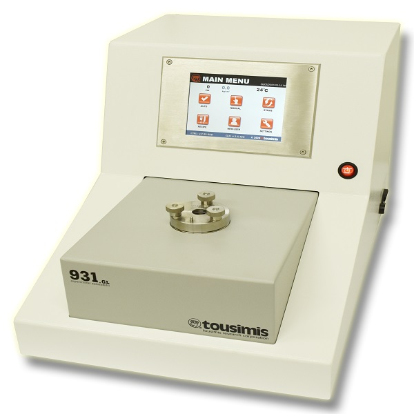
美国Tousimis电镜制样AUTOSAMDRI-931触摸屏全自动临界点干燥仪

二手-日本电子截面抛光仪 -JEOL IB-09010CP
上海林理仪器有限公司

基于机器学习的原位气体加热解决方案
上海微纳国际贸易有限公司

TEM Holder -真空转移TEM样品杆
勀杰科技有限公司

HITACHI 日立 扫描电镜灯丝 51E-0240
纳加霍里科技(内蒙古)有限公司