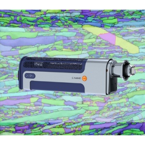
仪器种类: 台式/桌面型
电子枪种类: 钨灯丝
产地类别: 进口
二次电子图象分辨率: 1.0nm(15kV.WD=4mm)
放大倍数: 低:20-2,000x 高:100-500000x
加速电压: 1-30KV
背散射电子图像分辨率: 4nm@30kV(低真空模式)
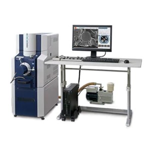
看了扫描电镜(SEM)的用户又看了
AZtecFeature是一种自动颗粒物分析系统,专门针对适用性和高速输出进行了优化。它结合了Ultim Max硅漂移探测器的高效性、灵敏性和Aztec优异的分析性能和简便操作,创造了先进的全自动颗粒物分析平台。
快速且强大
准确
操作简单
快速且强大
发挥新一代大面积Ultim Max SDD的潜力 - 在计数率低时实现高灵敏度,在计数率高时提供实现高效率
选择满足预算和测试需求的探测器
最多可装配4个探测器,以提供尽可能高的效率和灵敏度,并消除粗糙样品上的颗粒阴影
AZtec具有64位处理器,真正具有多任务处理能力
一个样品上至多可表征200,000个颗粒
实时检测,形貌和元素分析
在线或离线采集颗粒元素和相分析
采集数据同时进行分析和输出报告
准确
AZtecFeature采用Tru-Q技术,无需用户干预即可提供自动的元素识别和定量分析,使其成为理想的自动数据采集系统
改善的和峰修正可确保即使在高计数率下也能进行准确的定量分析
操作简单
即使对于新样品,也可以在几秒钟内获得结果——无需费力的设置程序
自动获得形貌和成分信息,并且易于匹配到颗粒分类中
完整的系统设置可以存储于用户账户中,并在以后调用
AZtecFeature在不同的专业领域有不同的应用:
1. 刑侦领域:AZtecGSR枪击残留物分析
AZtecGSR能在SEM中快速而准确地进行枪击残留物分析:它为 ASTM E1588 - 10e1 提供了可重复的枪击残留物分析结果。AZtecGSR结合了通过引导流程实现的易用性和使用Ultim Max探测器和 Tru-Q® 算法实现的高精度。
2.钢铁产业:AZtecSteel钢铁夹杂物分析
AZtecSteel是一种自动化的钢铁夹杂物分析软件包,利用扫描电子显微镜(SEM)中的能谱分析(EDS),专用于钢铁夹杂物的分析和分类,使SEM中的钢铁夹杂物分析变得更有效、更准确。它检测、测量并分析夹杂物,将数据结果按照公布的标准方法进行处理,并包含绘制复杂三元相图的功能。
3.矿物分析:AZtecMineral矿物分析软件
AZtecMineral是功能强大的自动化矿物解离分析解决方案。它利用多功能的扫描电镜进行矿物表征,并且为金属回收以及矿物产率的表征提供重要数据。同时,它是进行岩石表征的重要工具,可以代替耗时的光学显微镜分析。AZtecMineral可配备单个或多至四个牛津仪器大面积SDD能谱仪(Ultim Max),效率更高,在快速采集的同时进行准确矿物分类,以及其他多种功能分析。
4.增材制造:AZtecAM增材制造分析
AZtecAM是一个功能强大、自动化程度高的检测系统,专门用于分析增材制造(3D打印)中使用的金属原材料粉末。它在AZtecFeature平台的基础上优化了颗粒分析流程,以实现金属粉末的快速准确表征。AZtecAM自动检测和识别原材料粉末中杂质颗粒、记录粉末颗粒形貌特征,也可深入研究单个颗粒,提供从形貌到成分、单个到统计的所有信息,是确保完善的增材制造工艺和高品质产品的理想工具。
5.制造业清洁度分析:AZtecClean清洁度分析
AZtecClean是一个功能强大的自动化清洁度分析系统,专门用于制造业的清洁度控制。它利用AZtecFeature平台,自动实现对颗粒物的分析统计,快速表征制造工艺过程的杂质颗粒,控制清洁度。在汽车制造及供应链品质控制,航空制造业,发动机制造,锂电池原材料纯净度控制等领域有很强的应用,帮助提高制造工艺和品质。
半导体 2018-01-08

地矿 2018-01-08
能源/新能源 2018-01-08
钢铁/金属 2018-01-08
能源/新能源 2018-01-08
能源/新能源 2020-06-15
地矿 2018-01-08
地矿 2019-07-31
半导体 2018-01-08
半导体 2018-01-08
钢铁/金属 2018-01-08
钢铁/金属 2019-07-31
材料 2019-07-31
保修期: 详询工程师
是否可延长保修期: 是
现场技术咨询: 有
免费培训: 详询工程师
免费仪器保养: 详询工程师
保内维修承诺: 详询工程师
报修承诺: 详询工程师

牛津仪器INCAWave波谱仪
型号:WDS 135万
牛津仪器Ultim Extreme无窗超级能谱
型号:Ultim Extreme 20万 - 30万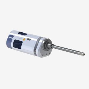
牛津仪器X-MaxTEM大面积硅漂移探测器
型号:Ultim Max TLE 50万 - 60万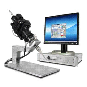
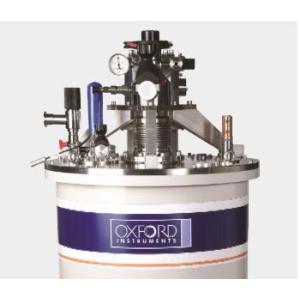
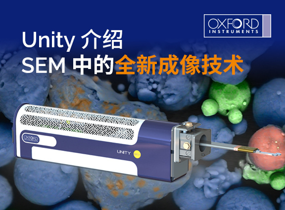
聚焦离子束扫描电镜用纳米操纵手 牛津仪器Omniprobe
型号:OmniProbe 100万 - 150万AZtecFeature是一种自动颗粒物分析系统,专门针对适用性和高速输出进行了优化。它结合了Ultim Max硅漂移探测器的高效性、灵敏性和Aztec出色的分析性能和简便操作,创造了先进的全自动颗粒物分析平台。
牛津仪器扫描电镜AZtecFeature的工作原理介绍
扫描电镜AZtecFeature的使用方法?
牛津仪器AZtecFeature多少钱一台?
扫描电镜AZtecFeature可以检测什么?
扫描电镜AZtecFeature使用的注意事项?
牛津仪器AZtecFeature的说明书有吗?
牛津仪器扫描电镜AZtecFeature的操作规程有吗?
牛津仪器扫描电镜AZtecFeature报价含票含运吗?
牛津仪器AZtecFeature有现货吗?

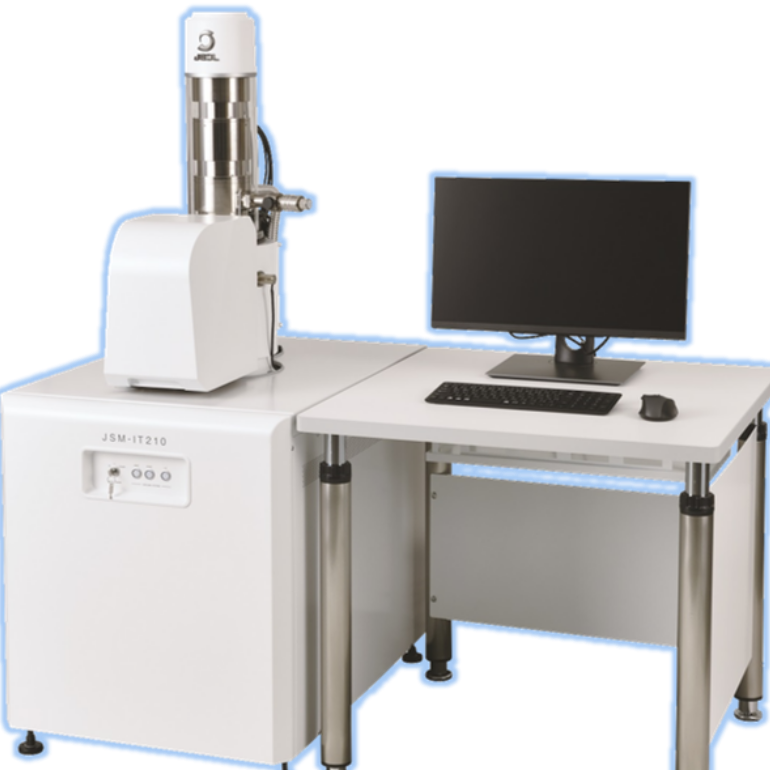
日本电子JEOL扫描电镜(SEM)JCM-7000
上海百贺仪器有限公司

电子扫描显微镜
昆山威天电子有限公司

JXA-8530F Plus 场发射EPMA
上海禹重实业有限公司

EM科特 CUBE-1000/1100台式桌面扫描电镜
广州领拓贸易有限公司