¥50万 - 100万
牛津仪器
暂无样本
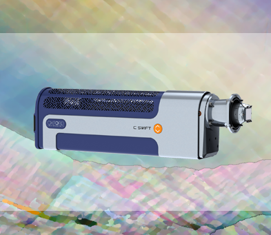
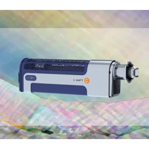
C-Swift
--
欧洲

产地类别: 进口
CCD相机分辨率: 1244×1024
极限速度: 870Hz
空间分辨率: 2nm
看了电子背散射衍射系统(EBSD)的用户又看了
C-Swift是CMOS探测器家族的新成员,专为常规材料分析和快速样品表征而设计。
C-Swift继承了Symmetry的许多优点,包括为EBSD专门定制CMOS传感器。这些优点使得C-Swift也成为一种开创性的EBSD探测器。
C-Swift是一个先进、高速EBSD探测器。与Symmetry探测器一样,C-Swift使用定制的CMOS传感器来实现高速和高灵敏度,以确保即使在更具挑战性的材料上也能获得高质量的结果。
C-Swift速度高达1000pps,同时可获得高质量的花样分辨率(156x128像素)。这相当于基于CCD的探测器以相似速度运行时所采集花样像素数的4倍,确保所有类型样品的可靠标定和高命中率。无失真光学系统与AZtec软件中强大的标定算法结合,使C-Swift能够提供优于0.05°的高角度精度。对于需要更高质量花样的应用, C-Swift可以以高达250pps的速度采集622x512像素的花样,使其成为复杂的多相样品和精细的相分析的理想选择。
这是专为快速、有效的样品表征而设计的探测器。系统的每个组件,从独特的接近传感器到可选的集成前置探测器,都经过设计, 旨在更大限度地提高性能和易用性, 并使EBSD成为每个实验室的标准工具。
确保1000 点/秒的标定速度
在250点/秒速度下,采集622x512像素的EBSD花样
对低能量和低束流分析具有非常高的灵敏度
无失真图像
当速度是关键时,C-Swift探测器达到了一个新标准:
仅需要12nA的电子束流,就能保证1000pps的标定速度
高速下的156x128像素的花样分辨率——同等速度下快速CCD探测器的4倍
全分辨率花样(622x512像素)——精细的相分析和形变分析的理想选择
低失真光学系统, 确保角度精度优于0.05°
优化的高灵敏度荧光屏, 确保低剂量和低束流能量下的高质量的花样——实现更大的空间分辨率
即使在快速下也能实现无缝的EDS集成
波纹管SEM接口,保持SEM真空完整性
独特的接近传感器——在可能发生的碰撞发生之前自动将探测器移动到安全位置
简单直观的探测器设置,确保每次都能获得良好的效果
五个集成的前置探测器, 提供全彩色通道衬度图像和原子序数衬度图像
半导体 2018-01-08
钢铁/金属 2020-06-15
半导体 2018-01-08
公安/司法 2018-01-08
半导体 2018-01-08
半导体 2018-01-08
公安/司法 2018-01-08
钢铁/金属 2020-06-15
保修期: 详询工程师
是否可延长保修期: 是
现场技术咨询: 有
免费培训: 详询工程师
免费仪器保养: 详询工程师
保内维修承诺: 详询工程师
报修承诺: 详询工程师

牛津仪器Ultim Extreme无窗超级能谱
型号:Ultim Extreme 20万 - 30万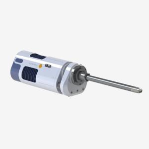
牛津仪器X-MaxTEM大面积硅漂移探测器
型号:Ultim Max TLE 50万 - 60万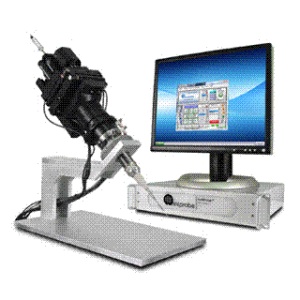
聚焦离子束扫描电镜用纳米操纵手 牛津仪器Omniprobe
型号:OmniProbe 100万 - 150万
电镜专用自动清洁度分析系统---牛津仪器AZtecFeature
型号:AZtecFeature 20万 - 30万牛津仪器 CMOS EBSD 电子背散射衍射仪 牛津仪器Symmetry探测器 / 牛津仪器C-Swift探测器 / 牛津仪器C-Nano探测器
牛津仪器EBSD系统C-Swift的工作原理介绍
EBSD系统C-Swift的使用方法?
牛津仪器C-Swift多少钱一台?
EBSD系统C-Swift可以检测什么?
EBSD系统C-Swift使用的注意事项?
牛津仪器C-Swift的说明书有吗?
牛津仪器EBSD系统C-Swift的操作规程有吗?
牛津仪器EBSD系统C-Swift报价含票含运吗?
牛津仪器C-Swift有现货吗?