


方案详情
文
介绍了在电介质和半导体薄膜叠层的情况下测量薄膜厚度的WLRS。所有的测量都是在400-1000nm光谱范围内用fr-basic进行的。反射探头的有效光斑直径为1毫米。样品为Si3N4/SiO2、聚Si/Si3N4/SiO2、PMMA/聚Si/Si3N4/SiO2组成的Si晶圆。在所有测量中,使用高反射镀铝镜(NT01-913-533,Edmund光学)进行参考测量。
方案详情

Film Metrology SpecialistsFor further information please contact us at info@thetametrisis.com or sales@thetametrisis.comThetaMetrisis C 2011, www.thetametrisis.com metrisis ThetaMetrisis APPLICATION NOTE #005 Thickness measurement of stack of films by White LightReflectance Spectroscopy (WLRS) Goal: The accurate measurement of the thickness of films in a stack consisting of 4 layers on asubstrate. Means & Methods: WLRS is introduced for the measurement of film thicknesses in the case of stack ofdielectric and semiconductor films. All measurements were performed with an FR-Basic in the 400-1000nmspectral regime. The reflection probe had an active spot size of 1mm in diameter. The sample was a Si waferwith areas consisting of SigN4 /SiO2, poly-Si /SigN4 /SiO2, PMMA/poly-Si /SigN4 /SiO2. In all measurements ahighly reflective Al coated mirror (NT01-913-533,Edmund Optics) was used for the reference measurements. Results: In fig. 1 the reflectance spectrum from a SigNa/SiO2 stack on Si wafer is shown. The calculatedthicknesses were: 576.63nm for SiOz and 127.78nm for the SigN4. In fig. 2 the reflectance spectrum from apoly-Si/SigN4/SiO2 stack on Si is shown. The calculated thicknesses were: 578.45nm for SiO2 and 144.77nm forthe SigN4 and 114.82nm for the polycrystalline Si. In fig. 3 the reflectance spectrum from a PMMA/poly-Si/SigN4/SiO2 stack (4 layers) on Si is shown. The calculated thicknesses were: 575.22nm for SiO2 and 147.57nmfor the SigN4, 115.73nm for the polycrystalline Si and 132.38nm for PMMA. The individual thickness of eachfilm is calculated simultaneously without any previous knowledge of the film thickness in all cases. In all cases,calculated film thicknesses were in very good agreement with the values obtained by spectroscopicellipsometry (<1% difference). - Scope-Darikk -Fited Spectrum -Scope-Dark-Fited Spectrur nlegrat negra sipoly_T(114.816nm)t (therm) (578.456 nmsi (Sopra Wavelength[nm] Wavelengh [nm] Figure 1: Typical reflectance spectrum from a SigN4/SiO2/Sisample (raw data without normalization). Black line:sample, Red line: fitting Figure 2: Typical reflectance spectrum from aa poly-Si/SigN4/SiOz/Si sample (raw data withoutnormalization). Black line: sample, Red line: fitting - Scoplipe Figure 3: Typical reflectance spectrum from aPMMA/poly-Si/SigNa/SiO2/Si sample (raw data without normalization). Black line: sample, Red line: fitting Conclusions: The thickness of at least 4 layers can be calculated simultaneously. 白光反射光谱法(WLRS)测量薄膜叠层厚度 目标:精确测量由4层组成的叠层中的薄膜厚度。方法和方法:介绍了在电介质和半导体薄膜叠层的情况下测量薄膜厚度的WLRS。所有的测量都是在400-1000nm光谱范围内用fr-basic进行的。反射探头的有效光斑直径为1毫米。样品为Si3N4/SiO2、聚Si/Si3N4/SiO2、PMMA/聚Si/Si3N4/SiO2组成的Si晶圆。在所有测量中,使用高反射镀铝镜(NT01-913-533,Edmund光学)进行参考测量。结果:在图1中,显示了Si3N4/SiO2叠层在Si晶片上的反射光谱。计算厚度:SiO2为576.63nm,Si3N4为127.78nm。在图2中,显示了在Si上的聚Si/Si3N4/SiO2叠层的反射光谱。计算厚度:SiO2为578.45nm,Si3N4为144.77nm,多晶Si为114.82nm。在图3中,显示了PMMA/聚-Si/Si3N4/SiO2叠层(4层)在Si上的反射光谱。计算厚度:SiO2为575.22nm,Si3N4为147.57nm,多晶Si为115.73nm,PMMA为132.38nm。在所有情况下,在不知道膜厚度的情况下,同时计算每个膜的单独厚度。在所有情况下,计算的薄膜厚度与光谱椭圆偏振法得到的值非常一致(<1%的差异)。结论:至少4层厚度可同时计算。FR的工具基于白光反射光谱(Reports) 。准确同步的厚度测量及薄膜的折射率-一个广泛的多样化的应用范围广泛的光电特性的工具和整体解决方案,如:半导体、有机电子、聚合物、涂料和涂料、光伏、生物传感、化学传感...
确定

还剩1页未读,是否继续阅读?

产品配置单


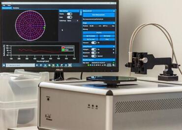
迈可诺技术有限公司为您提供《薄膜叠层中薄膜叠层厚度检测方案(白光干涉测厚)》,该方案主要用于电子元器件产品中薄膜叠层厚度检测,参考标准--,《薄膜叠层中薄膜叠层厚度检测方案(白光干涉测厚)》用到的仪器有扫描型光学膜厚仪 FR-Scanner、进口纳米狭缝涂布机、美国Laurell湿法刻蚀显影机EDC-650Mz-8NPP
相关方案
更多
该厂商其他方案
更多