


方案详情
文
For researchers of SWNTs, we offer the NanoLog® and Nanosizer®. Researchers of quantum dots can use our Fluorolog . For OLED technology, we have TCSPC instruments to resolve fluorescent lifetimes. HORIBA Jobin Yvon has the optimum spectrofluorometer for nanotechnology research in all these areas.
方案详情

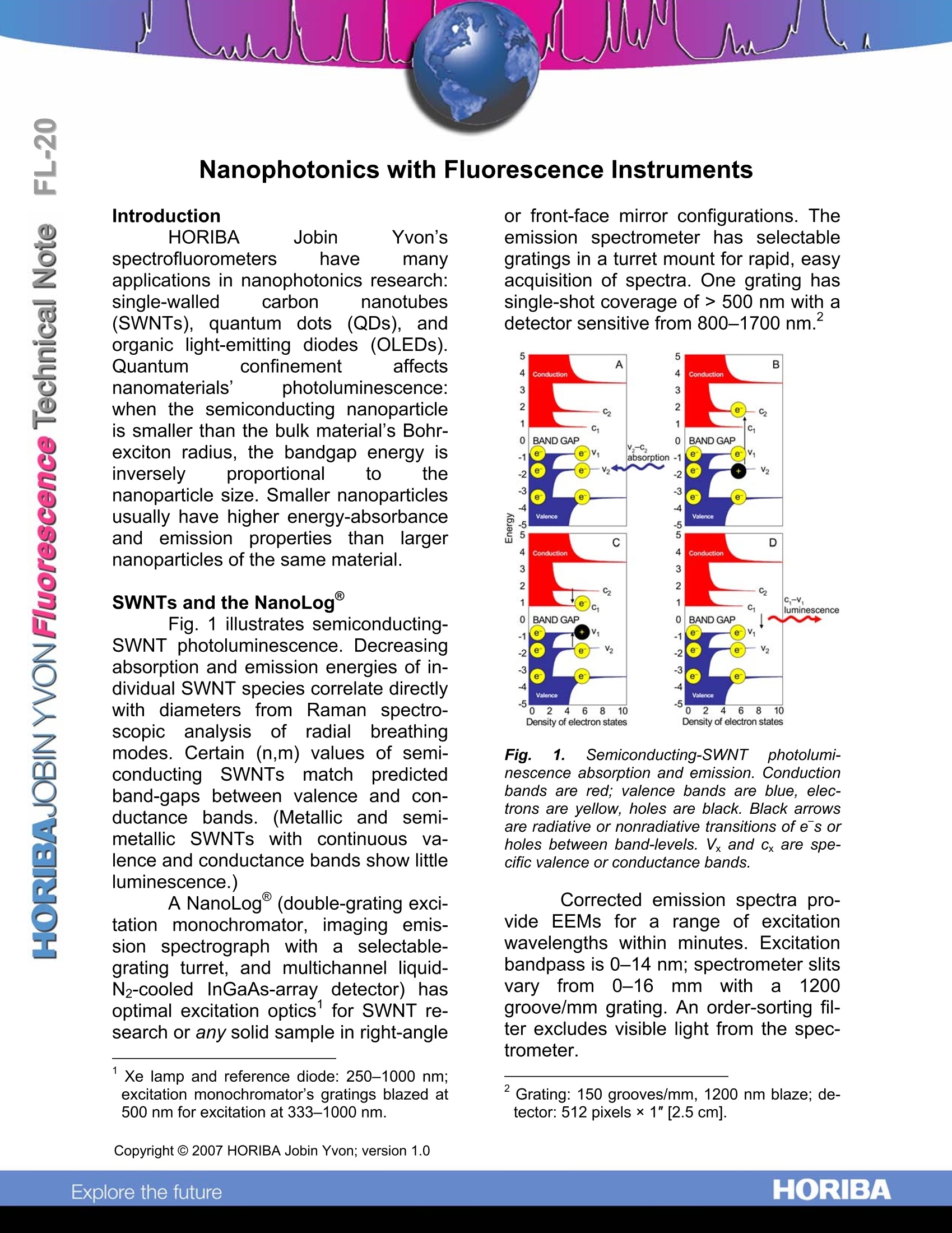
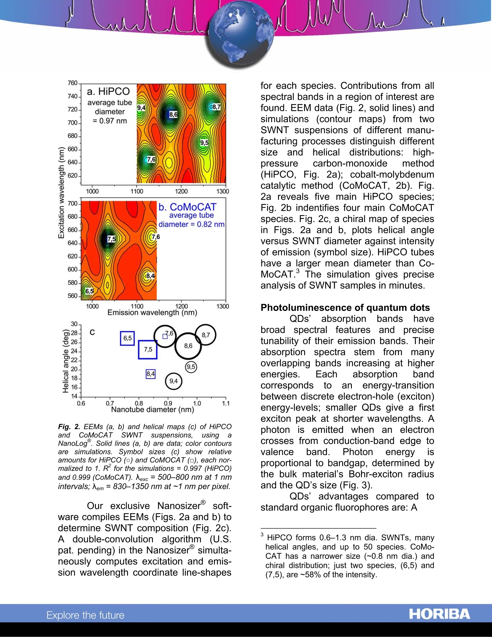
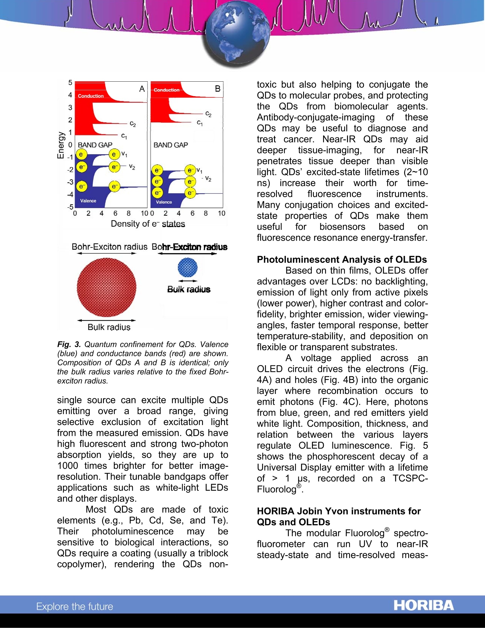
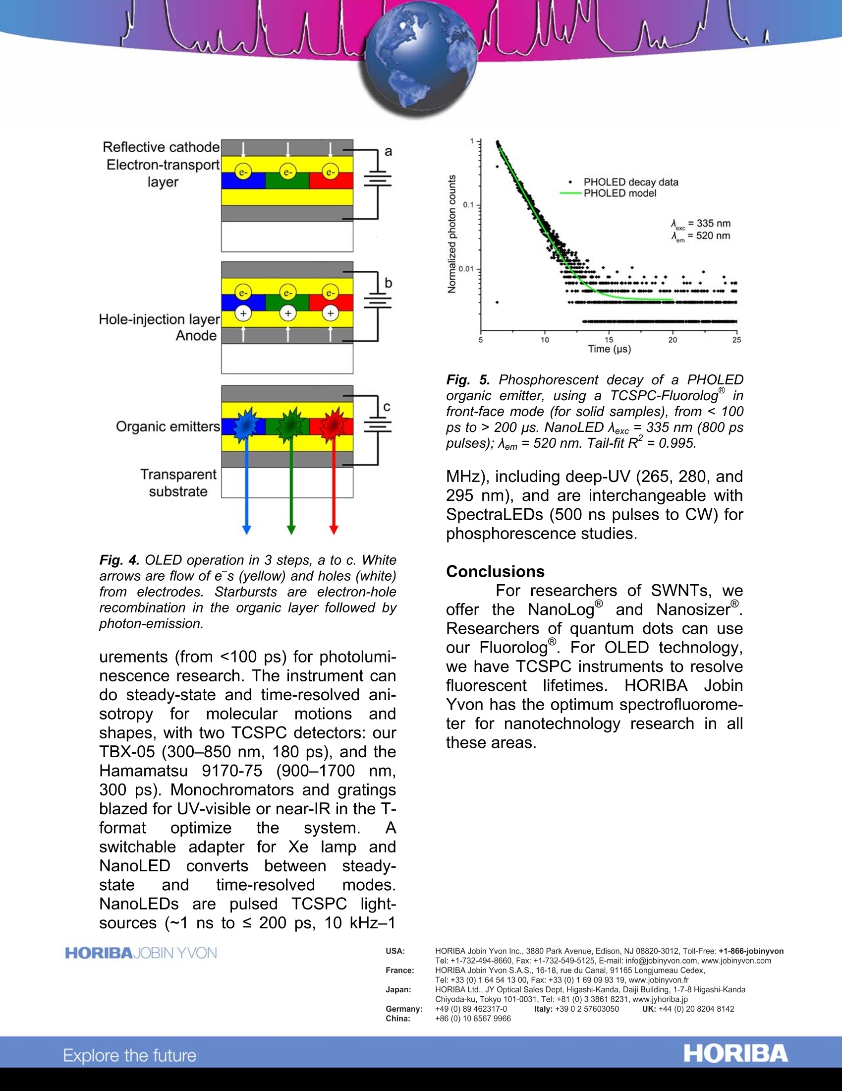
Nanophotonics with Fluorescence Instruments Introduction HORIBA Jobin Yvon'sspectrofluorometers have manyapplications in nanophotonics research:single-walled carbon nanotubes(SWNTs), quantum dots (QDs), andorganic light-emitting diodes (OLEDs).Quantum confinement affectsnanomaterials’ photoluminescence:when the semiconducting nanoparticleis smaller than the bulk material's Bohr-exciton radius, the bandgap energy isinversely proportional to thenanoparticle size. Smaller nanoparticlesusually have higher energy-absorbanceand emission properties than largernanoparticles of the same material. SWNTs and the NanoLog Fig. 1 illustrates semiconducting-SWNT photoluminescence. Decreasingabsorption and emission energies of in-dividual SWNT species correlate directlywith diameters from Raman spectro-scopice analysis ofrradial breathingmodes. Certain (n,m) values of semi-conductingSWNTsmatchpredictedband-gaps between valence and con-ductance bands. (Metallic and semi-metallic SWNTs with continuouss vva-lence and conductance bands show littleluminescence.) ANanoLog@(double-grating exci-tation monochromator, imaging emis-sion spectrographwith aselectable-grating turret, and multichannel liquid-N2-cooled InGaAs-array detector) hasoptimal excitation optics for SWNT re-search or any solid sample in right-angle ( Xe lamp and reference diode: 250-1000 nm;excitation monochromator's g r atings b l azed a t 500 nm for excitation a t 333-1000 nm. ) or front-face mirror configurations. Theemission spectrometer has selectablegratings in a turret mount for rapid, easyacquisition of spectra. One grating hassingle-shot coverage of > 500 nm with adetector sensitive from 800-1700 nm. Fig. 1. Semiconducting-SWNTphotolumi-nescence absorption and emission. Conductionbands are red; valence bands are blue, elec-trons are yellow, holes are black. Black arrowsare radiative or nonradiative transitions of e s orholes between band-levels. V and cx are spe-cific valence or conductance bands. Corrected emission spectra pro-vide EEMs for a range of excitationwavelengths within minutes. Excitationbandpass is 0-14 nm; spectrometer slitsvary/ from 0-16 mm)with1 a 1200groove/mm grating. An order-sorting fil-ter excludes visible light from the spec-trometer. ( ‘Grating: 150 grooves/mm, 1200 n m blaze; d e -tector: 512 pixels ×1"[2.5 cm]. ) 760 740. a. HiPCO 0.6 0.7 0.8 0.9 1.0 1.1 Nanotube diameter (nm) Fig. 2. EEMs (a, b) and helical maps (c) of HiPCOand CoMoCATSWNTsuspensions,usingaNanoLog. Solid lines (a, b) are data; color contoursare simulations. Symbol sizes (c) show relativeamounts for HiPCo (o)and CoMOCAT (口), each nor-malized to 1. R’ for the simulations=0.997 (HiPCO)and 0.999 (CoMoCAT). 入exc=500-800 nm at 1 nmintervals;Nem=830-1350 nm at~1 nm per pixel. Our exclusive Nanosizer soft-ware compiles EEMs (Figs. 2a and b) todetermine SWNT composition (Fig. 2c).A double-convolution algorithm (U.S.pat. pending) in the Nanosizer simulta-neously computes excitation and emis-sion wavelength coordinate line-shapes for each species. Contributions from allspectral bands in a region of interest arefound. EEM data (Fig.2, solid lines) andsimulations (contour maps) from ttwoSWNT suspensions of different manu-facturing processes distinguish differentsize and hehelliiccaall distributionss:: high-pressure carbon-monoxidenmethod(HiPCO, Fig. 2a); cobalt-molybdenumcatalytic method (CoMoCAT, 2b). Fig.2a reveals five main HiPCO species;Fig. 2b indentifies four main CoMoCATspecies. Fig. 2c, a chiral map of speciesin Figs. 2a and b, plots helical angleversus SWNT diameter against intensityof emission (symbol size). HiPCO tubeshave a larger mean diameter than Co-MoCAT.’ The simulation gives preciseanalysis of SWNT samples in minutes. Photoluminescence of quantum dots QDs’ absorptionbands havebroad spectralfeatures and precisetunability of their emission bands. Theirabsorption spectra stem from manyoverlapping bands increasing at higherenergies. Each absorption bandcorrespondstoani energy-transitionbetween discrete electron-hole (exciton)energy-levels; smaller QDs give a firstexciton peak at shorter wavelengths. Aphotonis emitted when an electroncrosses from conduction-band edge tovalenceband..PFhotonenergyi:isproportional to bandgap, determined bythe bulk material's Bohr-exciton radiusand the QD's size (Fig.3). QDs’ advantages compared tostandard organic fluorophores are: A ( ° HiPCO f orms 0 .6-1.3 nm d ia. SWNTs, m any helical angles, an d up t o 50 species. CoMo-CAT has a n a rrower size (~0.8 n m dia.) andchiral distribution; just two species, (6,5) and(7,5), are ~58% of the i n tensity. ) Bohr-Exciton radius Bohr-Exciton radius Fig. 3. Quantum confinement for QDs. Valence(blue) and conductance bands (red) are shown.Composition of QDs A and B is identical; onlythe bulk radius varies relative to the fixed Bohr-exciton radius. single source can excite multiple QDsemitting over a broad range, givingselective exclusion of excitation lightfrom the measured emission. QDs havehigh fluorescent and strong two-photonabsorption yields, so they are up to1000 times brighter for better image-resolution. Their tunable bandgaps offerapplications such as white-light LEDsand other displays. Most QDs are made of toxicelements (e.g., Pb, Cd, Se, anId Te).Theirphotoluminescencemay besensitive to biological interactions, soQDs require a coating (usually a triblockcopolymer), rendering the QDs non- toxic but also helping to conjugate theQDs to molecular probes, and protectingQDs from biomolecular agents.Antibody-conjugate-imaging offftheseQDs may be useful to diagnose andtreat cancer.. Near-IR QDs may aiqdeepertissue-imaging,forrnrear-IRpenetrates tissue deeper than visiblelight. QDs’excited-state lifetimes (2~10ns) increasetheirr worthfortime-resolved fluorescence instrumentsMany conjugation choices and excited-state properties of QDss make themuseful for biosensorsS based onfluorescence resonance energy-transfer. Photoluminescent Analysis of OLEDs Based on thin films, OLEDs offeradvantages over LCDs: no backlighting,emission of light only from active pixels(lower power), higher contrast and color-fidelity, brighter emission, wider viewing-angles, faster temporal response, bettertemperature-stability, and deposition onflexible or transparent substrates. A voltage applied across anOLED circuit drives the electrons (Fig.4A) and holes (Fig. 4B) into the organiclayer where recombination occurs toemit photons (Fig. 4C). Here, photonsfrom blue, green, and red emitters yieldwhite light. Composition, thickness, andrelation between tthhee variouslayersregulate OLED luminescence. Fig. 5shows the phosphorescent decay of aUniversal Display emitter with a lifetimeof > 1 us, recorded onnaa TTCSPC-Fluorolog@. HORIBA Jobin Yvon instruments forQDs and OLEDs The modular Fluorologspectro-fluorometer canrun UV to near-IRsteady-state and time-resolved meas- Fig. 4. OLED operation in 3 steps, a to c. Whitearrows are flow of e s (yellow) and holes (white)from electrodes. Starbursts are electron-holerecombination in the organic layer followed byphoton-emission. urements (from <100 ps) for photolumi-nescence research. The instrument cando steady-state and time-resolved ani-sotrop/y for molecular motions andshapes, with two TCSPC detectors: ourTBX-05 (300-850 nm, 180 ps), and theHamamatsu 9170-75(900-1700 nm,300 ps). Monochromators and gratingsblazed for UV-visible or near-IR in the T-formatoptimize the system. Aswitchable adapter for Xe lamp andNanoLED)cconverts betweennsteady-state and time-resolved modes.NanoLEDs are pulsed TCSPC light-sources (~1 ns to ≤ 200 ps, 10 kHz-1 Fig. 5. Phosphorescent decay of a PHOLEDorganic emitter, using a TCSPC-Fluorologe infront-face mode (for solid samples), from < 100ps to > 200 us. NanoLED Aexc= 335 nm (800 pspulses); Aem =520 nm. Tail-fit R²=0.995. MHz), including deep-UV (265, 280, and295 nm), and are interchangeable withSpectraLEDs (500 ns pulses to CW) forphosphorescence studies. Conclusions For researchers of SWNTs, weoffer the NanoLog and NanosizerResearchers of quantum dots can useour Fluorolog. For OLED technology,we have TCSPC instruments to resolvefluorescent lifetimes.HORIBAJobinYvon has the optimum spectrofluorome-ter for nanotechnology research in allthese areas. ( USA: H ORIBA Jobin Yvon In c ., 3 8 80 Park Avenue, Edison, NJ 08 8 20-3012, Toll-Free:+1 - 866-jobinyvon Tel: +1-732-494-8660, F ax: + 1 - 732-549-5125, E - mail: info@jobinyvon.com,www.jobinyvon.com France: H ORIBA Jobin Yvon S . A . S., 1 6-18, rue du Canal , 91165 Longjumeau Cedex, ) ( T el: +33 ( 0) 1 64 54 1 3 0 0, Fax: +33 (0) 1 69 09 9 3 1 9, w ww.jobinyvon.fr ) CopyrightC HORIBA Jobin Yvon; version .HORIBAExplore the future HORIBAExplore the future For researchers of SWNTs, we offer the NanoLog® and Nanosizer®. Researchers of quantum dots can use our Fluorolog . For OLED technology, we have TCSPC instruments to resolve fluorescent lifetimes. HORIBA Jobin Yvon has the optimum spectrofluorometer for nanotechnology research in all these areas.
确定
还剩2页未读,是否继续阅读?

产品配置单
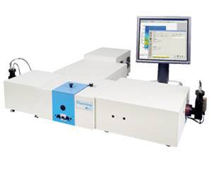
HORIBA(中国)为您提供《单壁碳纳米管,量子点,OLED中荧光检测方案(分子荧光光谱)》,该方案主要用于纳米材料中荧光检测,参考标准--,《单壁碳纳米管,量子点,OLED中荧光检测方案(分子荧光光谱)》用到的仪器有HORIBA Fluorolog®-3科研级荧光光谱仪
相关方案
更多
该厂商其他方案
更多