仪器种类: 维氏硬度计
测定材料: 金属硬度计
仪器类型: 台式
产地类别: 进口
测量范围: 10-100
总试验力: 0.5-50kgf
测试空间: 105/155mm (H) X 175 (D)
摄像头: 500万像素
看了硬度计的用户又看了
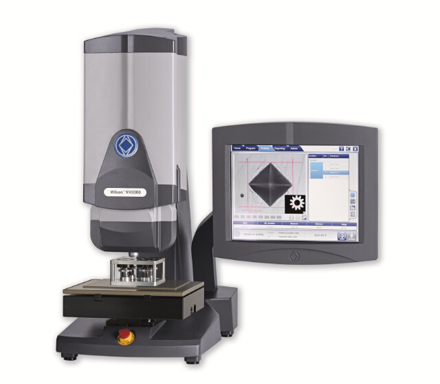
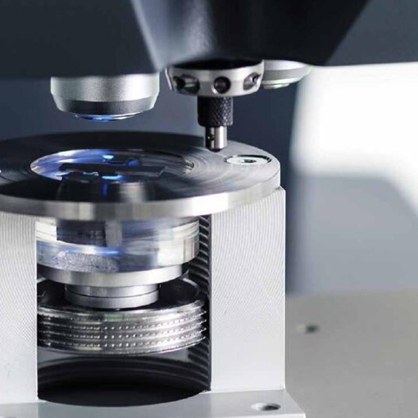
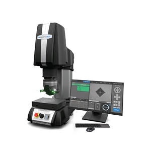
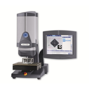
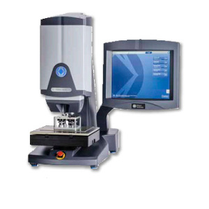
VH3300全自动维氏/努氏硬度计配备6位转塔,可同时安装3个力值传感器和3个压头,因此适用载荷范围非常宽,为10gf至50kgf。在配置 VH3300时,可根据您的测试需求,选择小型10N力值传感器、中型100N力值传感器或大型500N力值传感器。此外,加上Wilson DiaMet软件,按照ISO 6507、ISO 4545和ASTM E384标准要求,VH3300硬度计非常适合宏观维氏、显微维氏和努氏硬度测试。如果您只要求0.05—10kg载荷范围,不妨考虑一下我们的 VH3100硬度计!

通常在设置和操作时,自动化程度越高,复杂性也越高。DiaMet打破这一惯例,提供了快速、简单的操作,即使无经验的用户也能使用,同时还保留了专业用户 所需功能的灵活性及多样性。一旦设置好测试程序,操作者只需点击或触碰(触摸屏操作时)4下,即可运行该程序进行一系列维氏/努氏硬度测试。

防碰撞系统可检测到测试路径中的意外障碍物,从而防止压头或物镜因碰撞而损坏。在测试过程中,对运动系统进行持续监测,如果探测到障碍物,系统将立即停止运动。防碰撞系统为操作者提供了一项无与伦比、独特的重要安全优势,同时减少停机时间和维护费用。

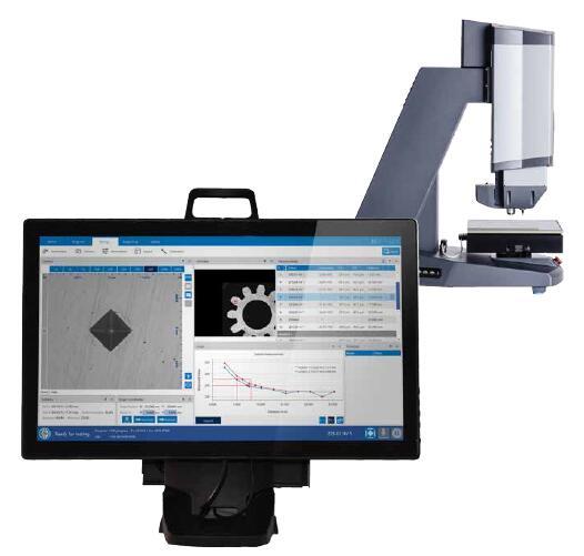
利用DiaMet™程序编辑功能,用户可以通过多种不同的变量创建任意数量的测试程序。精确度高,而且可以预览。同一程序可以创建不同的测试类型,并且可以将不同的测试力编入同一程序中。整个测试程序将自动运行。打压之前,操作者可以预览将要打点的位置。DiaMet软件具有视频叠加功能,这在测试多条程序时非常有用,可以避免重复打点。
自动照明
重现、重现、再重现; DiaMet自动照明功能可以不受材质类型(钢、工具钢、碳化物、涂层)的影响,根据样品的表面情况自动调整到合适的状态。
自动聚焦功能非常强大!软件可以轻松地从30mm或更远处对焦。当近距离聚焦时,可实现剪切式的自动聚焦速度。DiaMet自动聚焦算法树立了行业新标准。
采用精确的自动测量算法,无需手动测量。但是,仍可手动调整卡线位置。还可根据需要,对维氏和努氏硬度压痕对称性进行自动检查。
核实图表和网格中的测试结果,根据需要重新测量或重新打压。将结果导出到PDF、打印机或Excel。

| 威尔逊 VH3300产核心参数 | |
| 载荷 | 0.01-50kgf 可配置 |
| 物镜 | 3 位 - 可配置物镜 |
| 压头 | 多达3 位,努氏和维氏 |
| 全景相机 | 可选 |
| 测试标尺 | HV0.01 - HV0.025 - HV0.05 - HV0.1 - HV0.2 - HV0.1 - HV0.2 - HV0.3 - HV0.5 - HV1 - HV2 - HV3 - HV5 - HV10 - HV20 - HV30 - HV50 HK0.01 - HK0.025 - HK0.05 - HK0.1 - HK0.2 - HK0.3 - HK0.5 - HK1 - HK2 |
期待您的垂询!
依工测试测量仪器(上海)有限公司
标乐 Buehler & 威尔逊 Wilson 厂家
钢铁/金属 2009-09-18
电子/电气 2008-01-15

电子/电气 2007-01-19
医疗/卫生 2022-10-20
医疗/卫生 2022-10-20
医疗/卫生 2022-10-20
医疗/卫生 2022-10-20

医疗/卫生 2022-10-20
材料 2023-09-18
材料 2021-04-02
材料 2023-08-28

汽车及零部件 2022-06-14

汽车及零部件 2022-10-20

汽车及零部件 2024-05-09
电子/电气 2008-01-15
电子/电气 2007-01-19
钢铁/金属 2009-09-18
保修期: 1年
是否可延长保修期: 是
现场技术咨询: 有
免费培训: 面议
免费仪器保养: 面议
保内维修承诺: 面议
报修承诺: 面议
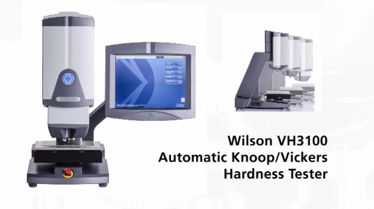
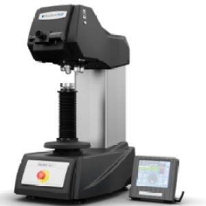
Wilson® VH3100 自动维氏/努氏硬度计
型号:VH3100 50万 - 100万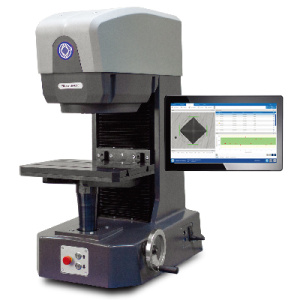
多功能硬度计 UH4000 | 美国威尔逊硬度计 Wilson
型号:Wilson ® UH4250 50万 - 100万
DiaMet 硬度测试软件
型号:Wilson DiaMet 50万 - 100万
维氏/努氏硬度计VH1102/1202 | 美国威尔逊硬度计
型号:VH1102/VH1202 20万 - 50万威尔逊 Wilson 硬度值转换表,您可以通过此表查询相关内容,也可以打印后张贴使用。如您需要纸质版,欢迎致电标乐咨询。
威尔逊硬度计VH3300的工作原理介绍
硬度计VH3300的使用方法?
威尔逊VH3300多少钱一台?
硬度计VH3300可以检测什么?
硬度计VH3300使用的注意事项?
威尔逊VH3300的说明书有吗?
威尔逊硬度计VH3300的操作规程有吗?
威尔逊硬度计VH3300报价含票含运吗?
威尔逊VH3300有现货吗?

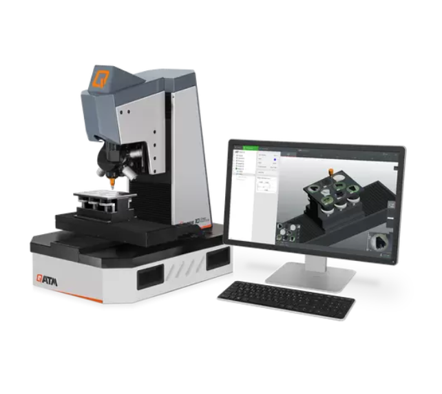
奥德镁QATM全自动显微硬度计 QNESS CHD MASTER+

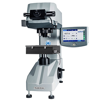
维氏/努氏硬度计VH1102/1202 | 美国威尔逊硬度计

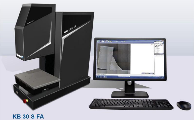
德国KB硬度计-全自动显微硬度计-维氏硬度计KB30S

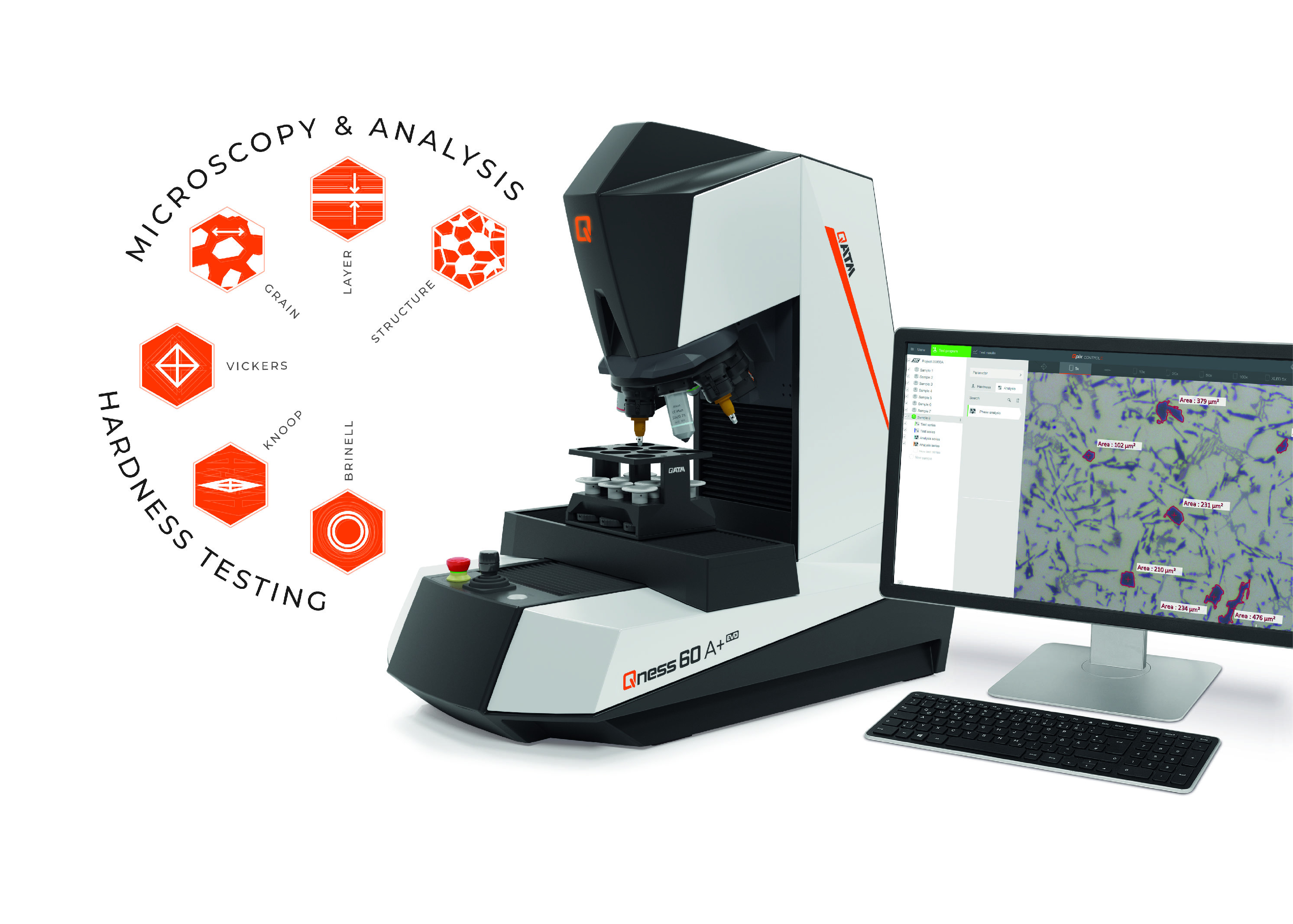
QATM Qness 60 A/A+ EVO 全自动显微硬度计

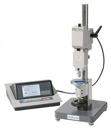
德国博锐 digi test Ⅱ全功能型硬度计

便携式里氏硬度计 数显模具钢材硬度检测仪DB22-HM450
厦门天合昆泰科技有限公司

德国厂家 BAREISS-- 数显水果硬度计二代 HPE II Fff
德商博锐仪器(上海)有限公司

9500系列万能硬度计
上海禹重实业有限公司

创佳CYHD-1固体原液酸奶食品硬度计面包面团硬度测试仪丸子硬度
烟台创佳智能科技有限公司